
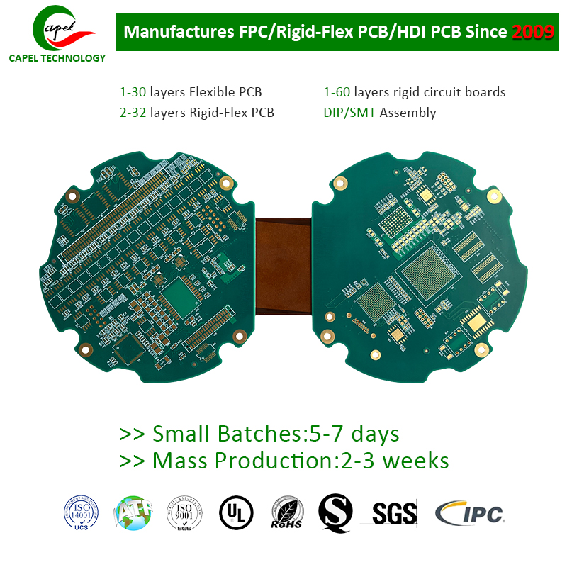
16-layer PCBs provide the complexity and flexibility required by modern electronic devices. Skilled design and selection of stacking sequences and interlayer connection methods are critical to achieving optimal board performance. In this article, we’ll explore considerations, guidelines, and best practices to help designers and engineers create efficient and reliable 16-layer circuit boards.
1.Understanding the Basics of 16 layer PCBs Stacking Sequence
1.1 Definition and purpose of stacking order
Stacking sequence refers to the arrangement and order in which materials such as copper and insulating layers are laminated together to form a multi-layer circuit board.The stacking sequence determines the placement of signal layers, power layers, ground layers, and other important components in the stack.
The main purpose of the stacking sequence is to achieve the required electrical and mechanical properties of the board. It plays a vital role in determining a circuit board’s impedance, signal integrity, power distribution, thermal management, and manufacturing feasibility. The stacking sequence also affects the overall performance, reliability, and manufacturability of the board.
1.2 Factors affecting stacking sequence design:There are several factors to consider when designing the stacking sequence of a
16-layer PCB:
a) Electrical considerations: The layout of signal, power, and ground planes should be optimized to ensure proper signal integrity, impedance control, and reduction of electromagnetic interference.
b) Thermal considerations: The placement of power and ground planes and the inclusion of thermal vias help to dissipate heat effectively and maintain the optimal operating temperature of the component.
c) Manufacturing constraints: The stacking sequence chosen should take into account the capabilities and limitations of the PCB manufacturing process, such as material availability, number of layers, drill aspect ratio, and alignment accuracy.
d) Cost Optimization: The selection of materials, number of layers, and stack-up complexity should be consistent with the project budget while ensuring the required performance and reliability.
1.3 Common types of 16-layer circuit board stacking sequences:There are several common stacking sequences for 16-layer
PCB, depending on the desired performance and requirements. Some common examples include:
a) Symmetric stacking sequence: This sequence involves placing signal layers symmetrically between power and ground layers to achieve good signal integrity, minimal crosstalk, and balanced heat dissipation.
b) Sequential stacking sequence: In this sequence, the signal layers are sequentially between the power and ground layers. It provides greater control over layer arrangement and is beneficial for meeting specific signal integrity requirements.
c) Mixed stacking order: This involves a combination of symmetric and sequential stacking orders. It allows customization and optimization of the layup for specific parts of the board.
d) Signal-sensitive stacking sequence: This sequence places sensitive signal layers closer to the ground plane for better noise immunity and isolation.
2.Key Considerations for 16 layer PCB Stacking Sequence Selection:
2.1 Signal integrity and power integrity considerations:
The stacking sequence has a significant impact on the signal integrity and power integrity of the board. Proper placement of signal and power/ground planes is critical to minimizing the risk of signal distortion, noise, and electromagnetic interference. Key considerations include:
a) Signal layer placement: High-speed signal layers should be placed close to the ground plane to provide a low-inductance return path and minimize noise coupling. Signal layers should also be carefully laid out to minimize signal skew and length matching.
b) Power plane distribution: The stacking sequence should ensure adequate power plane distribution to support power integrity. Sufficient power and ground planes should be strategically placed to minimize voltage drops, impedance discontinuities, and noise coupling.
c) Decoupling Capacitors: Proper placement of decoupling capacitors is critical to ensure adequate power transfer and minimize power supply noise. The stacking sequence should provide proximity and proximity of the decoupling capacitors to the power and ground planes.
2.2 Thermal management and heat dissipation:
Efficient thermal management is critical to ensuring circuit board reliability and performance. The stacking sequence should take into account the proper placement of power and ground planes, thermal vias, and other cooling mechanisms. Important considerations include:
a) Power plane distribution: Adequate distribution of power and ground planes throughout the stack helps direct heat away from sensitive components and ensures uniform temperature distribution across the board.
b) Thermal vias: The stacking sequence should allow for effective thermal via placement to facilitate heat dissipation from the inner layer to the outer layer or heat sink. This helps prevent localized hot spots and ensures efficient heat dissipation.
c) Component placement: Stacking sequence should consider the arrangement and proximity of heating components to avoid overheating. Proper alignment of components with cooling mechanisms such as heat sinks or fans should also be considered.
2.3 Manufacturing constraints and cost optimization:
The stacking sequence must take into account manufacturing constraints and cost optimization, as they play an important role in the feasibility and affordability of the board. Considerations include:
a) Material availability: The stacking sequence selected should be consistent with the availability of materials and their compatibility with the selected PCB manufacturing process.
b) Number of layers and complexity: The stacking sequence should be designed within the constraints of the selected PCB manufacturing process, taking into account factors such as number of layers, drill aspect ratio, and alignment accuracy.
c) Cost optimization: The stacking sequence should optimize the use of materials and reduce manufacturing complexity without compromising the required performance and reliability. It should aim to minimize costs associated with material waste, process complexity and assembly.
2.4 Layer alignment and signal crosstalk:
The stacking sequence should address layer alignment issues and minimize signal crosstalk that can negatively impact signal integrity. Important considerations include:
a) Symmetrical stacking: Symmetrical stacking of signal layers between power and ground layers helps minimize coupling and reduce crosstalk.
b) Differential pair routing: The stacking sequence should allow the signal layers to be properly aligned for efficient routing of high-speed differential signals. This helps maintain signal integrity and minimize crosstalk.
c) Signal separation: The stacking sequence should consider the separation of sensitive analog and digital signals to reduce crosstalk and interference.
2.5 Impedance control and RF/microwave integration:
For RF/microwave applications, the stacking sequence is critical to achieve proper impedance control and integration. Key considerations include:
a) Controlled impedance: The stacking sequence should allow for controlled impedance design, taking into account factors such as trace width, dielectric thickness, and layer arrangement. This ensures correct signal propagation and impedance matching for RF/microwave signals.
b) Signal layer placement: RF/microwave signals should be strategically placed close to the outer layer to minimize interference from other signals and provide better signal propagation.
c) RF Shielding: The stacking sequence should include proper placement of ground and shielding layers to isolate and protect RF/microwave signals from interference.
3.Interlayer Connection Methods
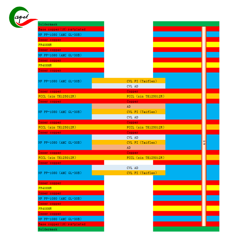
3.1 Through holes, blind holes and buried holes:
Vias are widely used in printed circuit board (PCB) design as a means of connecting different layers. They are drilled holes through all layers of the PCB and are plated to provide electrical continuity. Through holes provide a strong electrical connection and are relatively easy to make and repair. However, they require larger drill bit sizes, which take up valuable space on the PCB and limit routing options.
Blind and buried vias are alternative interlayer connection methods that offer advantages in space utilization and routing flexibility.
Blind vias are drilled from the PCB surface and terminate in inner layers without passing through all layers. They allow connections between adjacent layers while leaving deeper layers unaffected. This allows for more efficient use of board space and reduces the number of drill holes. Buried vias, on the other hand, are holes that are completely enclosed within the inner layers of the PCB and do not extend to the outer layers. They provide connections between inner layers without affecting the outer layers. Buried vias have greater space-saving advantages than through-holes and blind vias because they do not take up any space in the outer layer.
The choice of through holes, blind vias, and buried vias depends on the specific requirements of the PCB design. Through holes are typically used in simpler designs or where robustness and repairability are primary concerns. In high-density designs where space is a critical factor, such as handheld devices, smartphones, and laptops, blind and buried vias are preferred.
3.2 Micropore and HDI technology:
Microvias are small diameter holes (usually less than 150 microns) that provide high-density interlayer connections in PCBs. They offer significant advantages in miniaturization, signal integrity and routing flexibility.
Microvias can be divided into two types: through-hole microvias and blind microvias. Microvias are constructed by drilling holes from the top surface of the PCB and extending through all layers. Blind microvias, as the name suggests, only extend to specific internal layers and do not penetrate all layers.
High-density interconnect (HDI) is a technology that uses microvias and advanced manufacturing techniques to achieve higher circuit density and performance. HDI technology allows for the placement of smaller components and tighter routing, resulting in smaller form factors and higher signal integrity. HDI technology offers several advantages over traditional PCB technology in terms of miniaturization, improved signal propagation, reduced signal distortion, and enhanced functionality. It allows multilayer designs with multiple microvias, thereby shortening interconnect lengths and reducing parasitic capacitance and inductance.
HDI technology also enables the use of advanced materials such as high-frequency laminates and thin dielectric layers, which are critical for RF/microwave applications. It provides better impedance control, reduces signal loss and ensures reliable high-speed signal transmission.
3.3 Interlayer connection materials and processes:
The selection of interlayer connection materials and techniques is critical to ensuring good electrical performance, mechanical reliability and manufacturability of PCBs. Some commonly used interlayer connection materials and techniques are:
a) Copper: Copper is widely used in conductive layers and vias of PCBs due to its excellent conductivity and solderability. It is usually plated onto the hole to provide a reliable electrical connection.
b) Soldering: Soldering techniques, such as wave soldering or reflow soldering, are often used to make electrical connections between through holes on PCBs and other components. Apply solder paste to the via and apply heat to melt the solder and form a reliable connection.
c) Electroplating: Electroplating techniques such as electroless copper plating or electrolytic copper are used to plate vias to enhance conductivity and ensure good electrical connections.
d) Bonding: Bonding techniques, such as adhesive bonding or thermocompression bonding, are used to join layered structures together and create reliable interconnections.
e) Dielectric material: The choice of dielectric material for the PCB stackup is critical for interlayer connections. High frequency laminates such as FR-4 or Rogers laminates are often used to ensure good signal integrity and minimize signal loss.
3.4 Cross-sectional design and meaning:
The cross-sectional design of the PCB stackup determines the electrical and mechanical properties of the connections between layers. Key considerations for cross-section design include:
a) Layer arrangement: The arrangement of signal, power, and ground planes within a PCB stackup affects signal integrity, power integrity, and electromagnetic interference (EMI). Proper placement and alignment of signal layers with power and ground planes helps minimize noise coupling and ensure low inductance return paths.
b) Impedance control: Cross-section design should take into account controlled impedance requirements, especially for high-speed digital or RF/microwave signals. This involves appropriate selection of dielectric materials and thicknesses to achieve the desired characteristic impedance.
c) Thermal management: The cross-section design should consider effective heat dissipation and thermal management. Proper placement of power and ground planes, thermal vias, and components with cooling mechanisms (such as heat sinks) help dissipate heat and maintain optimal operating temperatures.
d) Mechanical reliability: Section design should consider mechanical reliability, especially in applications that may be subjected to thermal cycling or mechanical stress. Proper selection of materials, bonding techniques, and stackup configuration help ensure the structural integrity and durability of the PCB.
4.Design Guidelines for 16-Layer PCB
4.1 Layer allocation and distribution:
When designing a 16-layer circuit board, it is important to carefully allocate and distribute the layers to optimize performance and signal integrity. Here are some guidelines for tier allocation
and distribution:
Determine the number of signal layers required:
Consider the complexity of the circuit design and the number of signals that need to be routed. Allocate enough signal layers to accommodate all required signals, ensuring adequate routing space and avoiding excessive congestion. Assign ground and power planes:
Assign at least two inner layers to ground and power planes. A ground plane helps provide a stable reference for signals and minimizes electromagnetic interference (EMI). The power plane provides a low-impedance power distribution network that helps minimize voltage drops.
Separate sensitive signal layers:
Depending on the application, it may be necessary to separate sensitive or high-speed signal layers from noisy or high-power layers to prevent interference and crosstalk. This can be done by placing dedicated ground or power planes between them or using isolation layers.
Evenly distribute signal layers:
Distribute signal layers evenly throughout the board stackup to minimize coupling between adjacent signals and maintain signal integrity. Avoid placing signal layers next to each other in the same stackup area to minimize interlayer crosstalk.
Consider high-frequency signals:
If your design contains high-frequency signals, consider placing the high-frequency signal layers closer to the outer layers to minimize transmission line effects and reduce propagation delays.
4.2 Routing and signal routing:
Routing and signal trace design are critical to ensure proper signal integrity and minimize interference. Here are some guidelines for layout and signal routing on 16-layer circuit boards:
Use wider traces for high-current signals:
For signals that carry high current, such as power and ground connections, use wider traces to minimize resistance and voltage drop.
Matching impedance for high-speed signals:
For high-speed signals, ensure that the trace impedance matches the characteristic impedance of the transmission line to prevent reflections and signal attenuation. Use controlled impedance design techniques and correct trace width calculations.
Minimize trace lengths and crossover points:
Keep trace lengths as short as possible and reduce the number of crossover points to reduce parasitic capacitance, inductance, and interference. Optimize component placement and use dedicated routing layers to avoid long, complex traces.
Separate high-speed and low-speed signals:
Separate high-speed and low-speed signals to minimize the impact of noise on high-speed signals. Place high-speed signals on dedicated signal layers and keep them away from high-power or noisy components.
Use differential pairs for high-speed signals:
To minimize noise and maintain signal integrity for high-speed differential signals, use differential pair routing techniques. Keep the impedance and length of differential pairs matched to prevent signal skew and crosstalk.
4.3 Ground layer and power layer distribution:
Proper distribution of ground and power planes is critical to achieving good power integrity and reducing electromagnetic interference. Here are some guidelines for ground and power plane assignments on 16-layer circuit boards:
Allocate dedicated ground and power planes:
Allocate at least two inner layers for dedicated ground and power planes. This helps minimize ground loops, reduce EMI, and provide a low-impedance return path for high-frequency signals.
Separate digital and analog ground planes:
If the design has digital and analog sections, it is recommended to have separate ground planes for each section. This helps minimize noise coupling between the digital and analog sections and improves signal integrity.
Place ground and power planes close to signal planes:
Place ground and power planes close to the signal planes they feed to minimize loop area and reduce noise pickup.
Use multiple vias for power planes:
Use multiple vias to connect power planes to evenly distribute power and reduce power plane impedance. This helps minimize supply voltage drops and improves power integrity.
Avoid narrow necks in power planes:
Avoid narrow necks in power planes as they can cause current crowding and increase resistance, resulting in voltage drops and power plane inefficiencies. Use strong connections between different power plane areas.
4.4 Thermal pad and via placement:
Proper placement of thermal pads and vias is critical to effectively dissipating heat and preventing components from overheating. Here are some guidelines for thermal pad and via placement on 16-layer circuit boards:
Place thermal pad under heat-generating components:
Identify the heat-generating component (such as a power amplifier or high-power IC) and place the thermal pad directly beneath it. These thermal pads provide a direct thermal path to transfer heat to the internal thermal layer.
Use multiple thermal vias for heat dissipation:
Use multiple thermal vias to connect the thermal layer and outer layer to provide efficient heat dissipation. These vias can be placed in a staggered pattern around the thermal pad to achieve even heat distribution.
Consider thermal impedance and layer stackup:
When designing thermal vias, consider the thermal impedance of the board material and layer stackup.Optimize via size and spacing to minimize thermal resistance and maximize heat dissipation.
4.5 Component Placement and Signal Integrity:
Proper component placement is critical to maintaining signal integrity and minimizing interference. Here are some guidelines for placing components on a 16-layer circuit board:
Group related components:
Group related components that are part of the same subsystem or have strong electrical interactions. This reduces trace length and minimizes signal attenuation.
Keep high-speed components close:
Place high-speed components, such as high-frequency oscillators or microcontrollers, close to each other to minimize trace lengths and ensure proper signal integrity.
Minimize the trace length of critical signals:
Minimize the trace length of critical signals to reduce propagation delay and signal attenuation. Place these components as close as possible.
Separate sensitive components:
Separate noise-sensitive components, such as analog components or low-level sensors, from high-power or noisy components to minimize interference and maintain signal integrity.
Consider decoupling capacitors:
Place decoupling capacitors as close as possible to the power pins of each component to provide clean power and minimize voltage fluctuations. These capacitors help stabilize the power supply and reduce noise coupling.
5.Simulation and Analysis Tools for Stack-Up Design
5.1 3D modeling and simulation software:
3D modeling and simulation software is an important tool for stackup design because it allows designers to create virtual representations of PCB stackups. The software can visualize layers, components, and their physical interactions. By simulating the stackup, designers can identify potential issues such as signal crosstalk, EMI, and mechanical constraints. It also helps verify the arrangement of components and optimize the overall PCB design.
5.2 Signal integrity analysis tools:
Signal integrity analysis tools are critical for analyzing and optimizing the electrical performance of PCB stackups. These tools use mathematical algorithms to simulate and analyze signal behavior, including impedance control, signal reflections, and noise coupling. By performing simulation and analysis, designers can identify potential signal integrity issues early in the design process and make necessary adjustments to ensure reliable signal transmission.
5.3 Thermal analysis tools:
Thermal analysis tools play an important role in stackup design by analyzing and optimizing thermal management of PCBs. These tools simulate heat dissipation and temperature distribution within each layer of the stack. By accurately modeling power dissipation and heat transfer paths, designers can identify hot spots, optimize the placement of copper layers and thermal vias, and ensure proper cooling of critical components.
5.4 Design for manufacturability:
Design for manufacturability is an important aspect of stackup design. There are a variety of software tools available that can help ensure that the selected stack-up can be manufactured efficiently. These tools provide feedback on the feasibility of achieving the desired stackup, taking into account factors such as material availability, layer thickness, manufacturing process, and manufacturing cost. They help designers make informed decisions to optimize stacking to simplify manufacturing, reduce the risk of delays, and increase yields.
6.Step-by-Step Design Process for 16-Layer PCBs
6.1 Initial requirements collection:
In this step, gather all the necessary requirements for 16-layer PCB design. Understand the PCB’s functionality, required electrical performance, mechanical constraints, and any specific design guidelines or standards that need to be followed.
6.2 Component allocation and arrangement:
According to requirements, allocate components on the PCB and determine their arrangement. Consider factors such as signal integrity, thermal considerations, and mechanical constraints. Group components based on electrical characteristics and place them strategically on the board to minimize interference and optimize signal flow.
6.3 Stack-up design and layer distribution:
Determine the stack-up design for the 16-layer PCB. Consider factors such as dielectric constant, thermal conductivity, and cost to select the appropriate material. Assign signal, power, and ground planes according to electrical requirements. Place ground and power planes symmetrically to ensure a balanced stack and improve signal integrity.
6.4 Signal routing and routing optimization:
In this step, signal traces are routed between components to ensure proper impedance control, signal integrity, and minimize signal crosstalk. Optimize routing to minimize the length of critical signals, avoid crossing sensitive traces, and maintain separation between high-speed and low-speed signals. Use differential pairs and controlled impedance routing techniques when needed.
6.5 Interlayer connections and via placement:
Plan the placement of connecting vias between layers. Determine the appropriate via type, such as through hole or blind hole, based on layer transitions and component connections. Optimize via layout to minimize signal reflections, impedance discontinuities, and maintain even distribution on the PCB.
6.6 Final design verification and simulation:
Prior to manufacturing, final design verification and simulations are performed. Use simulation tools to analyze PCB designs for signal integrity, power integrity, thermal behavior, and manufacturability. Verify the design against initial requirements and make necessary adjustments to optimize performance and ensure manufacturability.
Collaborate and communicate with other stakeholders such as electrical engineers, mechanical engineers, and manufacturing teams throughout the design process to ensure all requirements are met and potential issues are resolved. Regularly review and iterate designs to incorporate feedback and improvements.
7.Industry Best Practices and Case Studies
7.1 Successful cases of 16-layer PCB design:
Case study 1: Shenzhen Capel Technology Co., Ltd. successfully designed a 16-layer PCB for high-speed network equipment. By carefully considering signal integrity and power distribution, they achieve superior performance and minimize electromagnetic interference. The key to their success is a fully optimized stack-up design using controlled impedance routing technology.
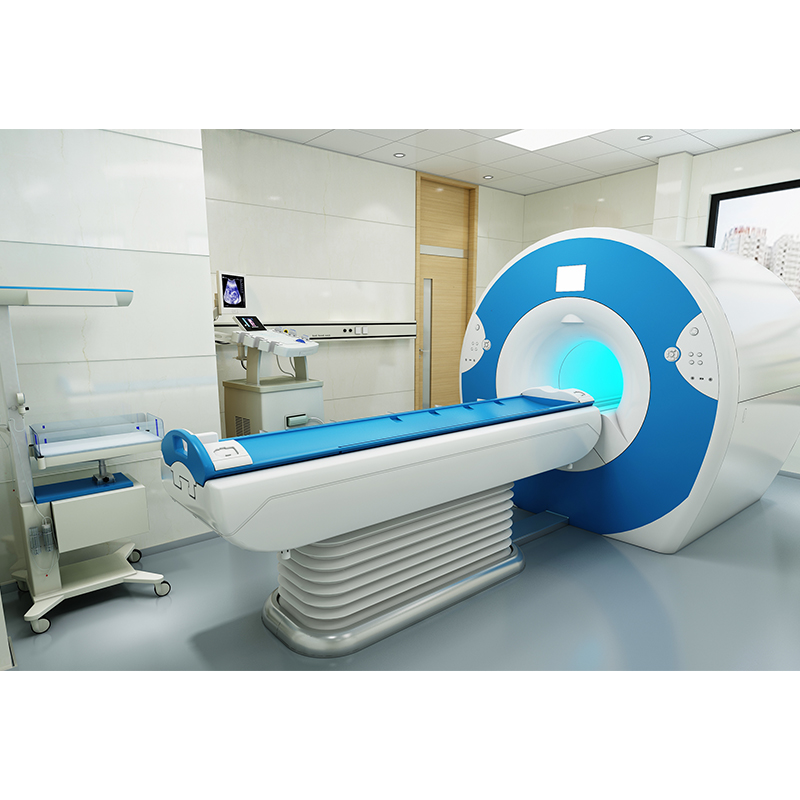
Case Study 2: Shenzhen Capel Technology Co., Ltd. designed a 16-layer PCB for a complex medical device. By using a combination of surface mount and through-hole components, they achieved a compact yet powerful design. Careful component placement and efficient routing ensure excellent signal integrity and reliability.
7.2 Learn from failures and avoid pitfalls:
Case Study 1: Some pcb manufacturers encountered signal integrity issues in the 16-layer PCB design of communications equipment. The reasons for failure were insufficient consideration of impedance control and lack of proper ground plane distribution. The lesson learned is to carefully analyze signal integrity requirements and enforce strict impedance control design guidelines.
Case Study 2: Some pcb makers faced manufacturing challenges with its 16-layer PCB due to design complexity. The overuse of blind vias and densely packed components leads to manufacturing and assembly difficulties. The lesson learned is to strike a balance between design complexity and manufacturability given the capabilities of the chosen PCB manufacturer.
To avoid pitfalls and pitfalls in 16-layer PCB design, it is crucial to:
a.Thoroughly understand the requirements and constraints of the design.
b.Stacked configurations that optimize signal integrity and power distribution. c.Carefully distribute and arrange components to optimize performance and simplify manufacturing.
d.Ensure proper routing techniques, such as controlling impedance and avoiding excessive use of blind vias.
e.Collaborate and communicate effectively with all stakeholders involved in the design process, including electrical and mechanical engineers and manufacturing teams.
f.Perform comprehensive design verification and simulation to identify and correct potential issues before manufacturing.
Post time: Sep-26-2023
Back


