
The impact of 4-layer circuit board routing and layer spacing on electromagnetic compatibility and signal integrity often creates significant challenges for engineers and designers. Effectively addressing these issues is critical to ensuring smooth operation and optimal performance of electronic devices. In this blog post, we will discuss how to solve the problem of the impact of 4-layer circuit board wiring and layer spacing on electromagnetic compatibility and signal integrity.
When it comes to the impact of 4-layer circuit board routing on electromagnetic compatibility (EMC) and signal integrity, one of the major concerns is potential crosstalk. Crosstalk is the unwanted coupling of electromagnetic energy between adjacent traces or components on a PCB, causing signal distortion and degradation. Proper insulation and spacing between traces can greatly reduce this problem.
To optimize EMC and signal integrity, it is critical to utilize design software that can perform accurate simulation and analysis. By using software tools such as electromagnetic field solvers, designers can evaluate the potential for crosstalk in virtual environments before proceeding with physical prototyping. This approach saves time, reduces costs, and improves overall design quality.
Another aspect to consider is the choice of PCB layup materials. The combination of the right dielectric material and the right thickness can significantly affect the electromagnetic behavior of a PCB. High-quality materials with low dielectric loss and controlled impedance properties help enhance signal integrity and reduce electromagnetic emissions.
Additionally, the layer spacing within a 4-layer circuit board can greatly affect EMC and signal integrity. Ideally, the spacing between adjacent PCB layers should be optimized to minimize electromagnetic interference and ensure proper signal propagation. Industry standards and design guidelines must be followed when determining the appropriate layer spacing for a specific application.
To address these challenges, the following strategies can be employed:
1. Careful component placement: Effective component placement helps reduce crosstalk on the PCB. By strategically placing components, designers can minimize the length of high-speed signal traces and reduce potential electromagnetic interference. This approach is especially important when dealing with critical components and sensitive circuits.
2. Ground layer design: Achieving a solid ground layer is an important technology to control EMC and improve signal integrity. The ground layer acts as a shield, reducing the spread of electromagnetic waves and preventing interference between different signal traces. It is important to ensure proper grounding techniques, including using multiple vias to connect ground planes on different layers.
3. Multilayer stackup design: Optimal stackup design involves choosing the appropriate layer sequence for signal, ground, and power layers. Carefully designed stackups help achieve controlled impedance, minimize crosstalk, and improve signal integrity. High-speed signals can be routed on the inner layer to avoid interference from external sources.
Capel’s expertise in enhancing EMC and signal integrity:
With 15 years of experience, Capel continues to improve its manufacturing processes and employ advanced technologies to optimize EMC and signal integrity. The highlights of Capel are as follows:
- Extensive Research: Capel invests in thorough research to identify emerging trends and challenges in PCB design to stay ahead of the curve.
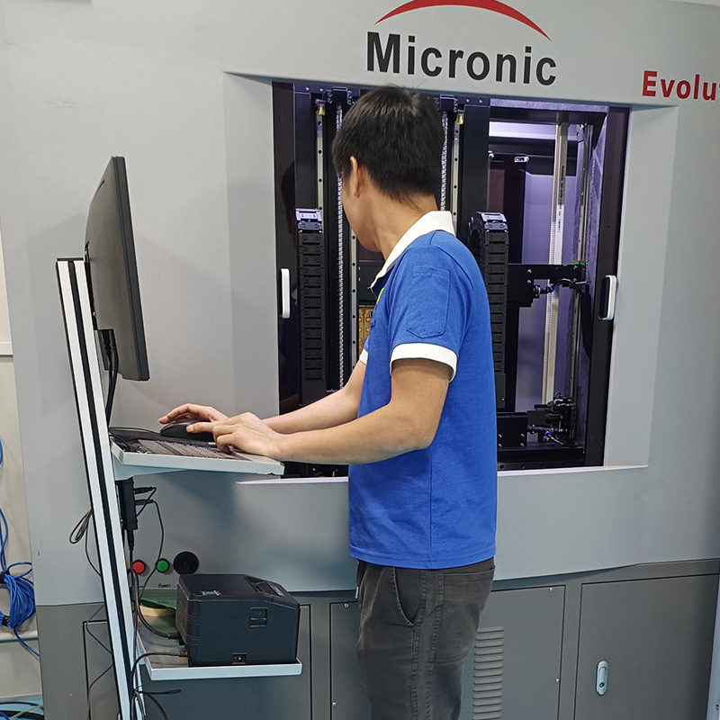
- State-of-the-art equipment: Capel utilizes state-of-the-art equipment to manufacture flexible PCBs and rigid-flex PCBs, ensuring the highest precision and quality.
- Skilled Professionals: Capel has a team of experienced professionals with deep expertise in the field, providing valuable insights and support for enhancing EMC and signal integrity.
In summary
Understanding the impact of 4-layer circuit board routing and layer spacing on electromagnetic compatibility and signal integrity is critical to successful electronic device design. By using advanced simulation, utilizing the right materials, and implementing effective design strategies, engineers can overcome these challenges and ensure overall PCB performance and reliability.With extensive experience and commitment to excellence, Capel remains a reliable partner in overcoming these challenges. By employing effective techniques in board layout, grounding and signal routing, while leveraging Capel’s expertise, designers can minimize EMI, enhance signal integrity, and build highly reliable and efficient boards.
Post time: Oct-05-2023
Back


