
The world of electronics has made tremendous progress in recent decades, and behind every electronic wonder lies a printed circuit board (PCB). These small but essential components are the backbone of nearly every electronic device. Different types of PCBs meet different requirements, one type is ENIG PCB. In this blog, we will delve into the details of the ENIG PCB, revealing its characteristics, uses and how it differs from other types of PCBs.
1.What is immersion gold PCB?
Here we will provides an in-depth look at ENIG PCBs, including their components, construction, and the electroless nickel immersion gold process used for manufacturing. Readers will clearly understand the unique features that make ENIG PCBs stand out.
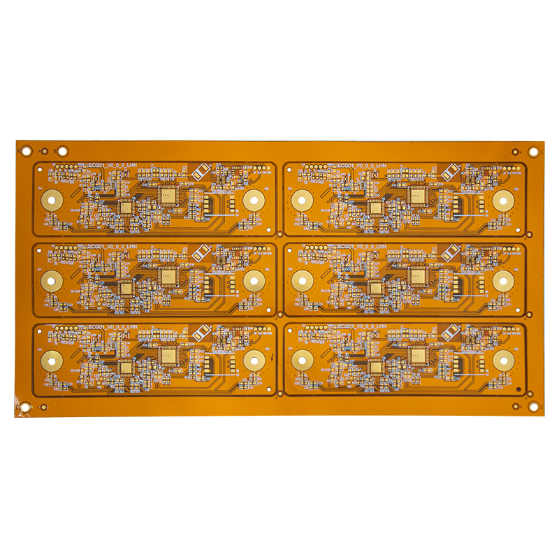
ENIG is the abbreviation of electroless nickel immersion gold plating, which is a commonly used surface treatment method in PCB manufacturing. It provides a reliable and cost-effective solution to ensure the longevity and performance of electronic equipment. ENIG PCBs are widely used in industries such as telecommunications, aerospace, consumer electronics, and medical devices.
ENIG PCBs are made up of three main components: nickel, gold, and a barrier layer. The barrier layer is usually made of a thin layer of electroless nickel deposited over the copper traces and pads of the PCB. This nickel layer acts as a diffusion barrier, preventing copper from migrating into the gold layer during gold deposition. After applying the nickel layer, a thin layer of gold is deposited on top. The gold layer provides excellent conductivity, durability and corrosion resistance. It also provides a level of protection against oxidation, ensuring long-term PCB performance and reliability.
The manufacturing process of ENIG PCB involves several steps. First, the PCB is surface treated and cleaned to remove contaminants and oxides from the copper surface. The PCB is then immersed in an electroless nickel plating bath, where a chemical reaction deposits a nickel layer onto the copper traces and pads. After the nickel is deposited, rinse and clean the PCB again to remove any remaining chemicals. Finally, the PCB is immersed in a gold bath and a thin layer of gold is plated on the nickel surface through a displacement reaction. The thickness of the gold layer can vary depending on the specific application and requirements. ENIG PCB offers several advantages over other surface treatments. One of the main advantages is its flat and uniform surface, which ensures excellent solderability and makes it suitable for Surface Mount Technology (SMT) assembly processes. Gold surfaces are also highly resistant to oxidation, helping to maintain reliable electrical connections over time.
Another benefit of ENIG PCBs is the ability to provide stable and consistent solder joints. The flat and smooth surface of the gold layer promotes good wetting and adhesion during the soldering process, resulting in a strong and reliable solder joint.
ENIG PCBs are also known for their superior electrical performance and signal integrity. The nickel layer acts as a barrier, preventing copper from diffusing into the gold layer and maintaining the electrical properties of the circuit. On the other hand, the gold layer has low contact resistance and excellent electrical conductivity, ensuring reliable signal transmission.
2.Benefits of ENIG PCB
Here we delve into the benefits of ENIG PCBs such as superior solderability, durability, corrosion resistance and electrical conductivity. These advantages make ENIG PCB suitable for a wide range of applications
ENIG PCB or Electroless Nickel Immersion Gold PCB offers several advantages over other surface treatments, making it suitable for a wide range of applications in the electronics industry. Let’s explore some of these advantages in more detail.
Excellent solderability:
ENIG PCBs have excellent solderability, making them ideal for Surface Mount Technology (SMT) assembly processes. The gold layer on top of the nickel barrier provides a flat and uniform surface, promoting good wetting and adhesion during soldering. This results in a strong, reliable solder joint, ensuring the overall integrity and performance of the PCB assembly.
Durability:
ENIG PCBs are known for their durability and longevity. The gold layer acts as a protective coating, providing a degree of protection against oxidation and corrosion. This ensures that the PCB can withstand harsh environmental conditions, including high humidity, temperature changes and exposure to chemicals. The durability of ENIG PCBs means greater reliability and longer life, making them suitable for applications requiring long-term performance.
Corrosion Resistance:
The electroless nickel layer in ENIG PCB creates a barrier between the copper traces and the gold layer. This barrier prevents copper from migrating into the gold during gold deposition. Therefore, ENIG PCB exhibits excellent corrosion resistance even in corrosive environments. This makes them ideal for applications where PCBs may be exposed to moisture, chemicals or other corrosive agents.
Conductivity:
ENIG PCB is highly conductive thanks to its gold layer. Gold is an excellent conductor of electricity and can transmit signals efficiently on PCBs. The uniform gold surface also ensures low contact resistance, minimizing any potential signal loss or degradation. This makes ENIG PCB suitable for applications requiring high-speed and high-frequency signal transmission, such as telecommunications, aerospace and consumer electronics.
Surface Flatness:
ENIG PCBs have a flat and uniform surface, which is critical for a consistent and reliable assembly process. The flat surface ensures even distribution of solder paste during stencil printing, thereby improving solder joint quality. It also facilitates precise placement of surface mount components, reducing the risk of misalignment or short circuits. The surface flatness of ENIG PCBs increases overall manufacturing efficiency and results in higher quality PCB assemblies.
Wire Bonding Compatibility:
ENIG PCBs are also compatible with the wire bonding process, where delicate wires are bonded to the PCB to make electrical connections. The gold layer provides a very suitable surface for wire bonding, ensuring a strong and reliable wire bond. This makes ENIG PCBs an excellent choice for applications requiring wire bonding, such as microelectronics, automotive electronics and medical devices.
RoHS Compliance:
ENIG PCBs are environmentally friendly and compliant with the Restriction of Hazardous Substances (RoHS) directive. The ENIG deposition process does not involve any harmful substances, making it a safer and more environmentally friendly alternative to other surface treatments that may contain toxic substances.
3.ENIG PCB vs. other types of PCB
A comprehensive comparison with other common PCB types such as FR-4, OSP, HASL and Immersion Silver PCB will highlight the unique attributes, advantages and disadvantages of each PCB.
FR-4 PCB: FR-4 (Flame Retardant 4) is a widely used PCB substrate material. It is an epoxy resin reinforced with woven glass fibers and is known for its good electrical insulating properties. FR-4 PCB has the following features:
advantage:
Good mechanical strength and rigidity
Excellent electrical insulation
Cost effective and widely available
shortcoming:
Not suitable for high frequency applications due to high dielectric loss
Limited thermal conductivity
Easily absorbs moisture over time, causing impedance changes and signal attenuation
In applications requiring high-frequency signal transmission, ENIG PCB is preferred over FR-4 PCB because ENIG offers better electrical performance and lower signal loss.
OSP PCB: OSP (Organic Solderability Preservative) is a surface treatment applied to PCBs to protect copper traces from oxidation. OSP PCB has the following features:
advantage:
Environmentally friendly and RoHS compliant
Lower cost compared to other surface treatments
Good for smoothness and flatness
shortcoming:
Relatively low shelf life; protective layer degrades over time
Limited resistance to moisture and harsh environments
Limited thermal resistance
When corrosion resistance, durability and extended service life are critical, ENIG PCB is preferred over OSP PCB due to ENIG’s superior oxidation and corrosion protection.
Spray tin PCB: HASL (Hot Air Solder Leveling) is a surface treatment method in which the
PCB is immersed in molten solder and then leveled with hot air. HASL PCB has the following features:
advantage: Cost effective and widely available
Good solderability and coplanarity
Suitable for through hole components
shortcoming:
The surface is uneven and there are potential coplanarity issues
Thick coatings may not be compatible with fine pitch components
Susceptible to thermal shock and oxidation during reflow soldering
ENIG PCBs are preferred over HASL PCBs for applications that require excellent solderability, flatter surfaces, better coplanarity, and compatibility with fine-pitch components.
Immersion silver PCB: Immersion silver is a surface treatment method in which a PCB is immersed in a silver bath, creating a thin layer of silver over the copper traces. Immersion Silver PCB has the following characteristics:
advantage:
Excellent electrical conductivity and solderability
Good flatness and coplanarity
Suitable for fine pitch components
shortcoming:
Limited shelf life due to tarnishing over time
Sensitive to handling and contamination during assembly
Not suitable for high temperature applications
When durability, corrosion resistance and extended shelf life are required, ENIG PCB is preferred over immersion silver PCB because ENIG has higher resistance to tarnishing and better compatibility with high temperature applications.
4.Application of ENIG PCB
ENIG PCB (i.e. Electroless Nickel Immersion Gold PCB) is widely used in various industries due to its various advantages over other types of PCB.This section explores the various industries using ENIG PCBs, emphasizing their importance in consumer electronics, aerospace and defense, medical devices, and industrial automation.
Consumer electronics products:
ENIG PCBs play a vital role in consumer electronics where compact size, high-speed performance and reliability are critical. They are used in smartphones, tablets, laptops, game consoles, and other electronic devices. ENIG’s excellent conductivity and low insertion loss make it ideal for high-frequency applications, enabling faster data transfer rates, signal integrity, and reduced electromagnetic interference. In addition, ENIG PCBs offer good solderability, which is crucial during the assembly of complex electronic components.
Aerospace and Defense:
The aerospace and defense industry has stringent requirements for electronic systems due to harsh operating conditions, extreme temperatures and high reliability standards. ENIG PCBs are widely used in avionics, satellite systems, radar equipment and military grade electronics. ENIG’s exceptional corrosion resistance and durability make it suitable for extended service life in challenging environments. Additionally, its uniform thickness and flatness ensure consistent performance and reliability.
Medical equipment:
In the medical field, ENIG PCBs are used in a wide range of applications, including patient monitoring systems, diagnostic equipment, imaging equipment, surgical instruments and implantable devices. ENIG’s biocompatibility and corrosion resistance make it suitable for medical devices that come into contact with body fluids or undergo sterilization processes. In addition, ENIG’s smooth surface and solderability allow precise connection and assembly of complex electronic components in medical devices. automated industry:
ENIG PCBs are widely used in industrial automation systems, including process control systems, robotics, motor drives, power supplies, and sensors. ENIG’s reliability and consistency make it an excellent choice for industrial applications that require continuous operation and resistance to harsh environments. ENIG’s excellent solderability ensures reliable connections in high power and high temperature applications, providing the necessary durability and stability for industrial automation systems.
Additionally, ENIG PCBs are used in other industries such as automotive, telecommunications, energy, and IoT (Internet of Things) devices. The automotive industry uses ENIG PCBs in vehicle electronics, engine control units, safety systems and entertainment systems. Telecom networks rely on ENIG PCBs to build base stations, routers, switches and communications equipment. In the energy sector, ENIG PCBs are used in power generation, distribution systems and renewable energy systems. Additionally, ENIG PCBs are an integral part of IoT devices, connecting various devices and enabling data exchange and automation.

5.ENIG PCB Manufacturing and Design Considerations
When designing and manufacturing ENIG PCBs, there are several important factors to consider to ensure optimal performance and reliability. Here are some key design guidelines and production processes specific to ENIG PCBs:
Pad design:
The pad design of the ENIG PCB is critical to ensure proper soldering and connection reliability. Pads should be designed with the correct dimensions, including width, length, and spacing, to accommodate component leads and solder paste. The pad surface finish should be smooth and clean to allow for proper wetting during the soldering process.
Trace width and spacing:
Trace width and spacing should comply with industry standards and PCB specific requirements. Ensuring the correct dimensions can prevent problems such as signal interference, short circuits, and electrical instability.
Board thickness and uniformity:
ENIG PCB consists of a layer of electroless nickel and an immersed gold layer. Plating thickness should be controlled within specific tolerances to ensure uniform coverage of the entire PCB surface. Uniform plating thickness is critical for consistent electrical performance and reliable solder joints.
Solder mask application:
Proper use of solder mask is critical to protecting PCB traces and preventing solder bridges. Solder mask should be applied evenly and accurately to ensure that the exposed pad has the required solder mask opening for soldering components.
Solder Paste Template Design:
When surface mount technology (SMT) is used for component assembly, solder paste stencils are used to accurately deposit solder paste onto the PCB pads. The stencil design should align correctly with the pad layout and allow precise deposition of solder paste to ensure proper solder joint formation during reflow.
Quality Control Check:
During the manufacturing process, it is important to perform quality control checks to ensure that the ENIG PCB meets the required specifications. These inspections may include visual inspection, electrical testing and solder joint analysis. Quality control checks help identify any issues during the production process and ensure that the finished PCB meets the required standards.
Assembly compatibility:
It is important to consider the compatibility of ENIG surface finishes with different assembly processes. The solderability and reflow characteristics of ENIG should be compatible with the specific assembly process used. This includes considerations such as solder paste selection, reflow profile optimization, and compatibility with lead-free soldering processes (if applicable).
By following these design guidelines and production processes for ENIG PCBs, manufacturers can ensure that the final product meets the required performance and reliability standards. It is important to work closely with PCB manufacturers and assembly partners to meet specific requirements and ensure the success of the manufacturing and assembly process.
6.ENIG PCB FAQ
What is ENIG PCB? What does it stand for?
ENIG PCB stands for Electroless Nickel Immersion Gold Printed Circuit Board. It is a commonly used surface treatment on PCBs and provides corrosion resistance, flatness and good solderability.
What are the benefits of using ENIG PCB?
ENIG PCBs offer several benefits, including excellent solderability, high electrical conductivity and corrosion resistance. The gold finish provides a layer of protection, making it suitable for applications where reliability is critical.
Is ENIG PCB expensive?
ENIG PCBs tend to be slightly more expensive compared to other surface treatments. The additional cost is due to the gold used in the soaking process. However, the advantages and reliability offered by ENIG make it the first choice for many applications, justifying its slightly higher cost.
Are there any restrictions on using ENIG PCB?
While ENIG PCBs have many advantages, they also have some limitations. For example, gold surfaces may wear easily if subjected to excessive mechanical stress or wear. Additionally, ENIG may not be suitable for applications with high temperature requirements or where certain harsh chemicals are used.
Is ENIG PCB easy to buy?
Yes, ENIG PCBs are widely available from various PCB manufacturers and suppliers. They are common finishing options and can be easily sourced to suit different project requirements. It is recommended to check availability and delivery times with the specific manufacturer or supplier.
Can I rework or repair the ENIG PCB?
Yes, ENIG PCBs can be reworked or repaired. However, the rework and repair process for ENIG may require special considerations and techniques compared to other surface treatments. It is recommended to consult an experienced PCB rework expert to ensure proper handling and avoid compromising the integrity of the gold surface.
Can ENIG be used for leaded and lead-free soldering?
Yes, ENIG can be used with leaded and lead-free soldering processes. However, it is critical to ensure compatibility with the specific solder paste and reflow profile used. In order to achieve reliable solder joints during assembly, welding parameters must be appropriately optimized.
The ENIG process is a reliable and cost-effective solution for manufacturers and electronics enthusiasts. The combination of a thin, evenly deposited nickel barrier and gold top layer provides an optimal surface finish to ensure the longevity and performance of electronic devices. Whether in telecommunications, aerospace or consumer electronics, ENIG PCBs continue to play a vital role in advancing technology and shaping the future of electronics.
Post time: Sep-13-2023
Back


