
In this blog post, we’ll explore the materials used in flexible PCBs and delve into the construction process, revealing the incredible technology behind these versatile circuit boards.
Flexible printed circuit boards (PCBs) have revolutionized the electronics industry by providing a flexible alternative to traditional rigid PCBs. Its unique construction and materials improve design flexibility, reliability and performance.
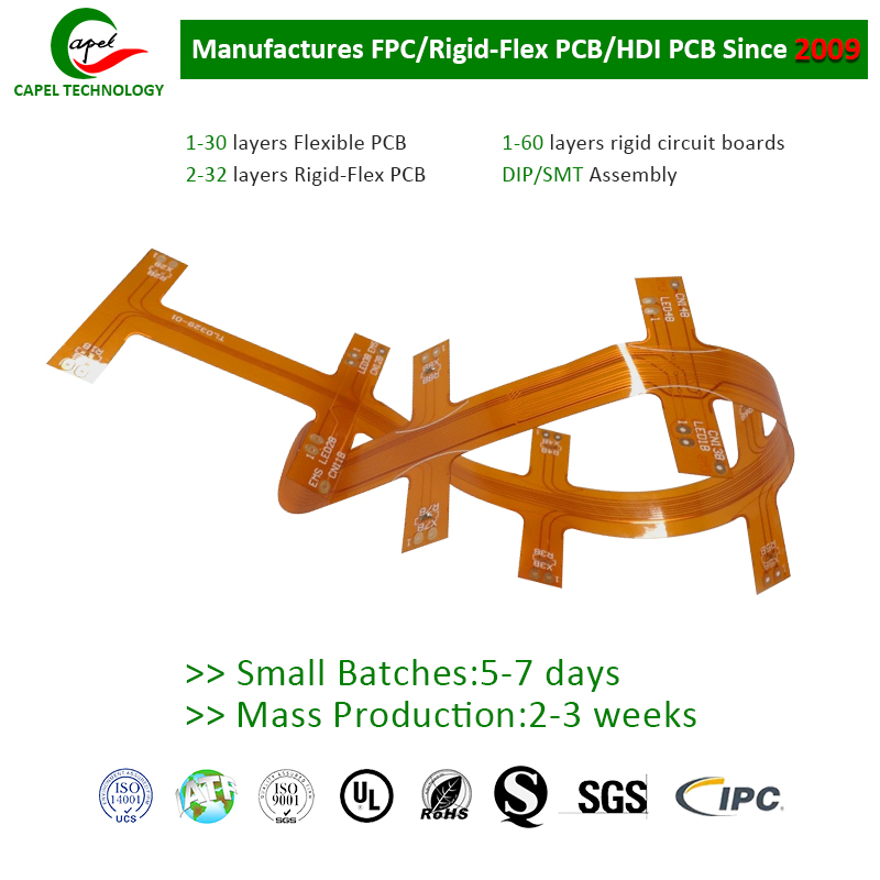
Materials used in flexible printed circuit boards
Flexible PCBs are made from a combination of different materials to increase their flexibility and durability. Let’s take a closer look at some of the key materials used in its construction:
1. Base material:
The foundation of any flexible PCB is the substrate material. Commonly used materials include polyimide (PI), a highly flexible and temperature-resistant polymer. PI has excellent mechanical strength, chemical resistance and insulation properties. Another popular substrate material is polyester (PET), which offers flexibility at a lower cost. These materials allow circuit boards to bend, twist and adapt to different shapes and sizes.
2. Conductive materials:
In order to establish electrical connections between different circuit elements, conductive materials such as copper are used. Copper is an excellent electrical conductor with good flexibility and is suitable for use in flexible printed circuit boards. Thin copper foil is laminated to the substrate to form the circuits and traces required for electrical connections.
3. Covering material:
The overlay material serves as a protective layer on the flexible PCB. They provide insulation, mechanical protection, and resistance to environmental factors such as moisture, dust, and chemicals. Polyimide overlays are widely used due to their excellent temperature stability, flexibility and durability.
Construction technology of flexible printed circuit boards
The construction process of a flexible PCB involves several different steps. Let’s explore each stage in detail:
1. Substrate preparation:
The first step in building a flexible PCB is to prepare the substrate material. The chosen substrate material, whether polyimide or polyester, is treated to enhance its surface roughness and adhesive properties. This treatment facilitates bonding of the conductive material to the substrate.
2. Circuit design and layout:
Next, use computer-aided design (CAD) software to create the circuit design and layout. Design determines the placement of electronic components on the circuit board and the routing of electrical connections. This step requires careful consideration of factors such as signal integrity, power distribution, and thermal management.
3. Etching and plating:
After the circuit design is completed, the etching process is performed on the substrate. Use a chemical solution to selectively remove excess copper, leaving the desired circuit traces and pads. After etching, the circuit board is plated with a thin layer of copper, which enhances the conductive path and ensures a stable electrical connection.
4. Solder mask and screen printing:
Solder mask is a protective layer that is applied to the surface of a circuit board. It protects copper traces from oxidation, solder bridging, and other external influences. It is then screen printed to add markings, such as component labels or polarity indicators, to facilitate assembly and troubleshooting.
5. Component installation and assembly:
Electronic components are mounted onto flexible PCBs using automated surface mount technology (SMT) machines or manual assembly techniques. Solder the components to the pads using soldering techniques such as reflow or wave soldering. Pay careful attention to ensure components are properly aligned and securely connected.
6. Testing and inspection:
Once the circuit board is assembled, it goes through a rigorous testing and inspection process to ensure its functionality and quality. Conduct automated tests such as In-Circuit Testing (ICT) or Automated Optical Inspection (AOI) to detect any potential defects or incorrect connections. These tests help identify and correct problems before the final product is shipped.
Flexible PCBs have become the first choice for applications where space constraints, weight reduction and flexibility are critical. Its unique materials and construction techniques allow for customization, reduced size and enhanced functionality. From the aerospace industry to medical devices and consumer electronics, flexible PCBs have left their mark in various fields.
In summary
Flexible PCBs offer a range of advantages due to their structure and materials. The combination of base material, conductive material and protective covering ensures flexibility, durability and reliability. Understanding the construction process of flexible printed circuit boards gives us insight into the incredible technology behind these versatile circuit boards. As technology continues to advance, flexible PCBs will continue to play a key role in shaping the future of the electronics industry.
Post time: Oct-11-2023
Back


