
In the field of electronics, circuit boards play a vital role in connecting various components and ensuring the smooth functioning of the device. Over the years, advances in technology have led to the development of more complex and compact circuit board designs. One such advancement is the introduction of HDI (High Density Interconnect) circuit boards. In this blog post, we will explore the differences between HDI circuit boards and regular PCB (Printed Circuit Board) boards.
Before delving into the specific content, let’s first understand the basic concepts of HDI circuit boards and PCB boards. A PCB is a flat plate made of non-conductive material with conductive pathways etched into it. These paths, also called traces, are responsible for carrying electrical signals between different components on the circuit board. PCB boards are widely used in a variety of electronic devices, from smartphones and laptops to medical equipment and automotive systems.
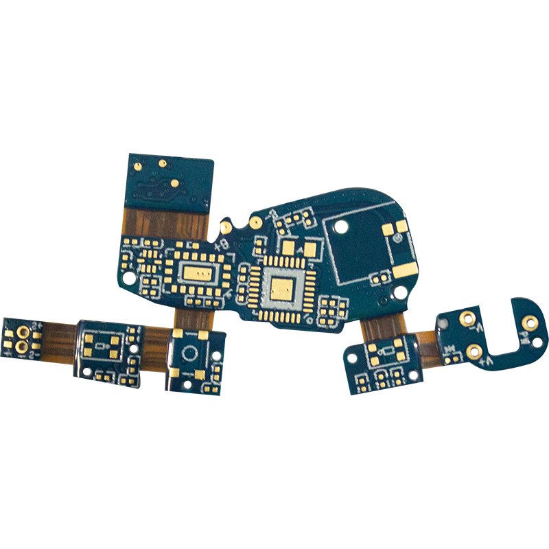
HDI boards, on the other hand, are more advanced versions of PCB boards. HDI technology allows for higher circuit density, thinner lines, and thinner materials. This enables the production of smaller, lighter and more robust electronic devices. HDI circuit boards are typically used in applications that require higher speed, better performance, and miniaturization, such as high-end smartphones, tablets, and aerospace equipment.
Now let’s take a look at the difference between HDI circuit boards and ordinary PCB boards:
Circuit Density and Complexity:
The main differentiating factor between HDI circuit boards and regular PCB boards is circuit density. HDI boards have significantly higher circuit density due to their advanced manufacturing techniques and specialized design rules. Compared to traditional PCB boards, which usually have fewer layers, HDI boards typically have more layers, ranging from 4 to 20 layers. They allow the use of additional layers and smaller vias, allowing more components to be integrated into a smaller space. On the other hand, ordinary PCB boards are limited by their simpler design and fewer layers, resulting in lower circuit density.
Micropore technology:
HDI circuit boards widely use microvia technology, including blind vias, buried vias and stacked vias. These vias provide direct connections between different layers, reducing the surface area required for routing and maximizing available space. In contrast, ordinary PCB boards often rely on through-hole technology, which limits their ability to achieve high circuit density, especially in multi-layer designs.
Advances in materials:
HDI circuit boards typically feature materials with enhanced thermal, electrical, and mechanical properties. These materials provide improved performance, reliability and durability, making HDI boards suitable for demanding applications. Regular PCB boards, while still functional, often use more basic materials and may not meet the stringent requirements of complex electronic devices.
Miniaturization:
HDI circuit boards are designed to meet the increasing miniaturization needs of electronic devices. Advanced manufacturing techniques used in HDI boards allow for smaller vias (holes that connect different layers) and finer traces. This results in a higher density of components per unit area, enabling the production of smaller, sleeker devices without compromising performance.
Signal integrity and high-speed applications:
As the demand for faster data transmission and higher signal integrity continues to grow, HDI circuit boards offer significant advantages over regular PCB boards. Reduced via and trace sizes in HDI boards minimize signal loss and noise interference, making them suitable for high-speed applications. HDI technology also allows for the integration of additional features such as blind and buried vias, further enhancing signal performance and reliability.
Manufacturing cost:
It is worth noting that the manufacturing cost of HDI circuit boards is usually higher compared to ordinary PCB boards. The increase in complexity and number of layers makes the manufacturing process more complex and time-consuming. Additionally, the use of advanced materials and specialized equipment adds to the overall cost. However, the advantages and performance improvements offered by HDI boards often outweigh their higher cost, especially in industries where high reliability and miniaturization are critical.
Applications and advantages:
Application of HDI circuit board:
HDI boards are widely used in compact electronic devices such as smartphones, tablets, wearable devices, and small medical devices. Their ability to support advanced functionality and shrink form factors makes them ideally suited for these applications.
Advantages of HDI circuit boards:
- Greater circuit density allows for more complex and feature-rich designs.
- Improved signal integrity due to reduced parasitic capacitance and inductance.
- Enhanced heat dissipation ensures optimal performance of high-power components.
- Smaller profile saves space and supports lightweight design.
- Improved resistance to shock, vibration and environmental factors, improving overall equipment reliability.
To sum up, the difference between HDI circuit boards and ordinary PCB boards is huge. HDI circuit boards offer superior circuit density, advanced manufacturing techniques and signal integrity advantages, making them ideal for high-performance, compact electronic devices. However, ordinary PCB boards can also function in applications that do not require high complexity or miniaturization. Understanding these differences will enable designers and manufacturers to select the appropriate circuit board for their specific needs, ensuring optimal functionality, reliability and performance for their electronic devices.
Post time: Sep-12-2023
Back


