
HDI (High Density Interconnect) rigid-flex PCBs represent the pinnacle of advanced printed circuit board technology, combining the advantages of high-density wiring capabilities with the flexibility of rigid-flex boards. This article aims to elucidate the manufacturing process of HDI rigid-flex PCB and provide valuable insights into its structure, materials and key manufacturing steps. By understanding the complexities involved, engineers and designers can optimize their designs and collaborate effectively with manufacturers to turn their innovative ideas into reality.
1.Understand HDI rigid flexible PCB:
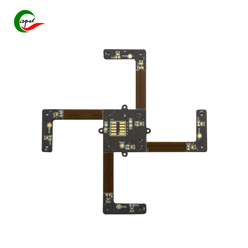
HDI (High Density Interconnect) rigid-flex PCB is an advanced form of printed circuit board that combines the advantages of high-density interconnection and flexibility. This unique combination makes them ideally suited to meet the requirements of modern electronic equipment.
High-density interconnection refers to the ability to achieve high-density components and signal routing within limited board space. As the demand for smaller, more compact devices continues to grow, HDI technology enables the design and production of complex circuits in smaller form factors. Increased interconnect density allows more functionality to be integrated into smaller devices, making them more efficient and powerful.
Flexibility is another key attribute of HDI rigid-flex PCBs. This flexibility allows the board to be bent, folded or twisted without affecting performance or reliability. Flexibility is especially beneficial for electronic devices that require complex physical designs or need to withstand vibration, shock, or extreme environments. It also enables seamless integration of electronic components from different circuit board sections, eliminating the need for additional connectors or cables.
Utilizing HDI technology offers several advantages. First, it greatly improves signal integrity by minimizing the distance between components and interconnects, reducing signal loss, crosstalk and electromagnetic interference. This enhances performance and reliability for high-speed digital and RF applications. Secondly, HDI rigid-flex PCB can significantly reduce the overall size and weight of electronic equipment. HDI technology eliminates the need for additional connectors, cables, and board-to-board connections, allowing for compact, lightweight designs. This is particularly valuable for industries such as aerospace and portable consumer electronics, where saving weight and space is critical. In addition, HDI technology also improves the reliability of electronic equipment. By minimizing the number of interconnects, HDI rigid-flex PCBs reduce the risk of failure due to loose connections or solder joint fatigue. This improves product quality and increases long-term reliability.
HDI rigid-flex applications are found in a variety of industries, including aerospace, medical devices, telecommunications and consumer electronics. In the aerospace industry, HDI rigid-flex PCBs are used in flight control systems, avionics, and communications systems because of their compact size, light weight, and ability to withstand extreme conditions. In the medical field, they are used in devices such as pacemakers, medical imaging systems, and implantable devices. Telecommunications and consumer electronics benefit from reduced size and improved performance of HDI rigid-flex PCBs in smartphones, tablets, wearables, and other portable devices.
2.HDI rigid-flexible PCB manufacturing process: step-by-step
A. Design constraints and prepare CAD files:
The first step in the HDI rigid-flex PCB manufacturing process is to consider the design constraints and prepare the CAD files. Design constraints play a critical role in determining PCB performance, reliability, and manufacturability. Some important design constraints to consider are:
Size Limitations:
The size of a PCB depends on the requirements of the device in which it is used. It is necessary to ensure that the PCB fits into the designated space without affecting functionality or reliability.
Reliability:
PCB design should be reliable and able to withstand expected operating conditions. Factors such as temperature, humidity, vibration and mechanical stress need to be considered during the design process.
Signal Integrity:
Designs should consider signal integrity to minimize the risk of signal attenuation, noise, or interference. High-speed digital and RF signals require careful routing and impedance control.
Thermal Management:
Thermal management is critical to preventing overheating and ensuring optimal performance of electronic components. Heat dissipation can be achieved through proper placement of thermal vias, heat sinks, and thermal pads. CAD software is used to create PCB layout files. It allows designers to define layer stacking, component placement and copper trace routing. CAD software provides the tools and capabilities to accurately represent and visualize designs, making it easier to identify and correct any potential problems before production.
B. Material Selection and Layup Design:
After preparing the CAD files, the next step is material selection and layup design. Choosing the right materials is critical to ensuring that HDI rigid-flex PCBs achieve the required electrical performance, thermal management, and mechanical integrity. Rigid layer materials, such as FR-4 or high-performance laminates, provide mechanical support and stability. The flexible layer is usually made of polyimide or polyester film for flexibility and durability. The stackup design process involves determining the arrangement of different layers, including rigid and flexible layers, copper thickness, and dielectric materials. The stackup design should consider factors such as signal integrity, impedance control, and power distribution. Proper layer placement and material selection help ensure efficient signal transmission, minimize crosstalk and provide necessary flexibility.
C. Laser drilling and microhole formation:
Laser drilling is a critical step in creating high-density routing microvias in HDI PCBs. Microvias are small holes used to connect different layers of a PCB, allowing for higher density interconnections. Laser drilling offers several advantages over traditional mechanical drilling methods. It allows for smaller apertures, allowing for higher routing density and more compact designs. Laser drilling also provides greater precision and control, reducing the risk of misalignment or damage to surrounding materials. In the laser drilling process, a focused laser beam is used to ablate material, creating small holes. The holes are then metallized to provide conductivity between the layers, allowing efficient transmission of signals.
D. Chemical copper plating:
Electroless copper plating is a key step in the manufacturing process of HDI rigid-flex boards. The process involves depositing a thin layer of copper within the micropores and on the surface of the PCB. The importance of electroless copper plating lies in its ability to ensure reliable electrical connections and good signal transmission. The copper layer fills the microvias and connects the different layers of the PCB, forming a conductive path for signals. It also provides a solderable surface for component attachment. The electroless copper plating process involves several steps, including surface preparation, activation and deposition. The PCB is first cleaned and activated to promote adhesion. A chemical reaction is then used to apply a solution containing copper ions to the PCB surface, depositing a thin layer of copper.
E. Image Transfer and Lithography:
Image transmission and photolithography are components of the HDI rigid-flex PCB manufacturing process. These steps include using a photoresist material to create a circuit pattern on the PCB surface and exposing it to UV light through a patterned photomask. During the image transfer process, photoresist material is applied to the PCB surface. Photoresist materials are sensitive to UV light and can be selectively exposed. The PCB is then aligned with the patterned photomask and UV light is passed through the clear areas of the photomask to expose the photoresist. After exposure, the PCB is developed to remove the unexposed photoresist, leaving the desired circuit pattern. These patterns act as protective layers in subsequent processes. To create circuit traces, etching chemicals are used to remove unwanted copper. Areas not covered by the photoresist are exposed to the etchant, which selectively removes the copper, leaving the desired circuit traces.
F. Etching and electroplating process:
The purpose of the etching process is to remove excess copper and create circuit traces on the HDI rigid-flex PCB. Etching involves using an etchant, usually an acid or chemical solution, to selectively remove unwanted copper. The etching is controlled by a protective photoresist layer that prevents the etchant from attacking the required circuit traces. Carefully control the duration and concentration of the etchant to achieve the desired trace width and depth. After etching, the remaining photoresist is stripped off to expose the circuit traces. The stripping process involves using solvents to dissolve and remove the photoresist, leaving clean and well-defined circuit traces. To reinforce circuit traces and ensure proper conductivity, a plating process is required. This involves depositing an additional layer of copper on the circuit traces through an electroplating or electroless plating process. The thickness and uniformity of copper plating are critical to achieving a reliable electrical connection.
G. Solder mask application and component assembly:
Solder mask application and component assembly are important steps in the HDI rigid-flex PCB manufacturing process. Use solder mask to protect copper traces and provide insulation between them. Solder mask forms a protective layer over the entire PCB surface, excluding areas that require soldering, such as component pads and vias. This helps prevent solder bridging and shorts during assembly. Component assembly involves placing electronic components onto a PCB and soldering them into place. Components are carefully positioned and aligned with the landing pad to ensure proper electrical connections. Use soldering techniques such as reflow or wave soldering depending on component type and assembly requirements. The reflow soldering process involves heating the PCB to a specific temperature that causes the solder to melt and form a permanent connection between the component leads and the PCB pads. Wave soldering is typically used for through-hole components, where the PCB is passed through a wave of molten solder to form a connection.
H. Testing and Quality Control:
The final step in the HDI rigid-flex PCB manufacturing process is testing and quality control. Rigorous testing is critical to ensure PCB performance, reliability and functionality. Perform electrical tests to check for shorts, opens, and continuity. This involves applying specific voltages and currents to the PCB and measuring the response using automated test equipment. Visual inspections are also performed to verify solder joint quality, component placement, and overall cleanliness of the PCB. It helps identify any potential defects such as misaligned components, solder bridges, or contaminants. In addition, thermal stress analysis can be performed to evaluate a PCB’s ability to withstand temperature cycling or thermal shock. This is especially important in applications where the PCB is exposed to extreme temperature changes. During and after each step of the manufacturing process, quality control measures are implemented to ensure that the PCB meets the required specifications and standards. This includes monitoring process parameters, conducting statistical process control (SPC), and performing periodic audits to identify and correct any deviations or anomalies.

3.Challenges faced in manufacturing HDI rigid-flex boards:
Manufacturing HDI rigid-flex boards presents some complexities and challenges that must be carefully managed to ensure a high-quality end product. These challenges revolve around three key areas: precise alignment, surface defects, and impedance changes during lamination.
Precise alignment is critical for HDI rigid-flex boards because they involve multiple layers and materials that must be positioned precisely. Achieving precise alignment requires careful handling and positioning of different layers to ensure vias and other components are properly aligned. Any misalignment can cause major problems such as signal loss, shorts, or breaks. Manufacturers must invest in advanced equipment and technology to ensure precise alignment throughout the production process.
Avoiding surface defects is another major challenge. During the manufacturing process, surface defects such as scratches, dents, or contaminants may occur, affecting the performance and reliability of HDI rigid-flex boards. These defects can interfere with electrical connections, affect signal integrity, or even cause the board to fail altogether. To prevent surface defects, strict quality control measures must be taken, including careful handling, regular inspections, and the use of a clean environment during production.
Minimizing impedance changes during lamination is critical to maintaining the electrical performance of HDI rigid-flex boards. Lamination involves using heat and pressure to bond different layers together. However, this process may cause changes in the dielectric constant and conductor width, resulting in undesirable impedance changes. Controlling the lamination process to minimize these changes requires precise control of temperature, pressure, and time, as well as strict adherence to design specifications. In addition, advanced testing and verification techniques can be employed to ensure that the required impedance is maintained.
Overcoming these challenges in manufacturing HDI flex boards requires designers and manufacturers to work closely together throughout the process. Designers need to carefully consider manufacturing constraints and effectively communicate them to manufacturers. On the other hand, manufacturers must understand the design requirements and constraints in order to implement a suitable manufacturing process. Collaboration helps address potential issues early in the design phase and ensures the manufacturing process is optimized for high-quality HDI rigid-flex boards.
Conclusion:
The manufacturing process of HDI rigid-flex PCB is a series of complex but critical steps that require skilled, precise and reliable technology. Understanding each stage of the process enables Capel to optimize their ability to deliver outstanding output within tight deadlines. By prioritizing collaborative design efforts, automation and continuous process improvement, Capel can stay at the forefront of HDI rigid-flex PCB manufacturing and meet the growing demand for multi-functional and high-performance boards across industries.
Post time: Sep-15-2023
Back


