
Rigid-flex printed circuit boards (PCBs) have gained immense popularity in the electronics industry due to their ability to combine the advantages of both rigid and flexible substrates. As these boards become more complex and densely populated, accurately calculating the minimum trace width and spacing becomes crucial for ensuring reliable performance and avoiding issues like signal interference and short circuits. This comprehensive guide will outline the essential steps to calculate the minimum trace width and spacing for rigid-flex PCB fabrication, enabling you to develop high-quality and durable PCB designs.
Understanding Rigid-Flex PCBs:
Rigid-flex PCB is a printed circuit board that combines rigid and flexible substrates on one board. These substrates are connected by plated through holes (PTHs), providing electrical connections between the rigid and flexible areas of the PCB. The rigid areas of the PCB are made of strong, non-flexible materials such as FR-4, while the flexible areas are made of materials such as polyimide or polyester. The flexibility of the substrate allows the PCB to be bent or folded to fit spaces not available with traditional rigid boards. Rigid-flex The combination of rigid and flexible areas in a PCB allows for a more compact and flexible design, making it suitable for applications with limited space or complex geometries. These PCBs are used in a wide variety of industries and applications, including aerospace, medical devices, automotive electronics, and consumer electronics. Rigid-flex PCBs offer several advantages over traditional rigid boards. They can reduce the size and weight of electronic equipment and simplify the assembly process by eliminating extra connectors and cables. They also offer better reliability and durability because there are fewer points of failure than traditional rigid boards.
Importance of Calculating rigid flex PCB fabrication Minimum Trace Width and Spacing:
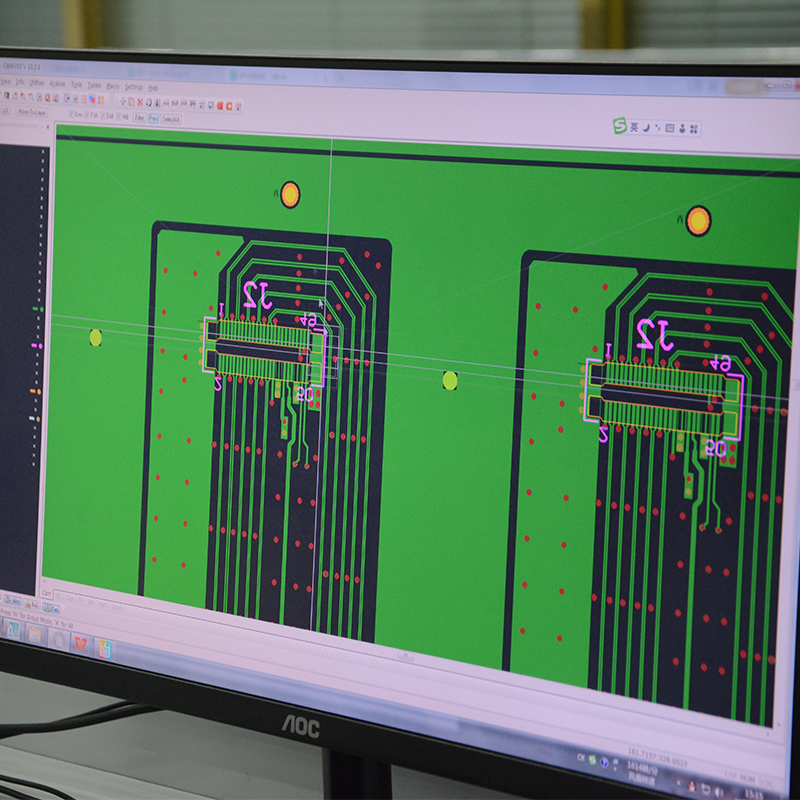
Calculating the minimum trace width and spacing is critical as it directly affects the electrical characteristics of the PCB design. Insufficient trace width can result in high resistance, limiting the amount of current that can flow through the trace. This can cause a voltage drop and power loss that can affect the overall functionality of the circuit. Insufficient trace spacing can lead to short circuits as adjacent traces may touch each other. This may cause electric leakage, which may damage the circuit and cause a malfunction. Additionally, insufficient spacing can lead to signal crosstalk, where a signal from one trace interferes with adjacent traces, reducing signal integrity and causing data transmission errors. Accurate calculation of minimum trace width and spacing is also critical to ensure manufacturability. PCB manufacturers have specific capabilities and constraints regarding trace fabrication and assembly processes. By adhering to minimum trace width and spacing requirements, you can ensure that your design can be successfully manufactured without issues such as bridging or opens.
Factors Affecting Rigid Flex PCB Fabrication Minimum Trace Width and Spacing:
Several factors affect the calculation of the minimum trace width and spacing for a rigid-flex PCB. These include current carrying capacity, operating voltage, dielectric material properties and isolation requirements. Other key factors include the manufacturing process used, such as manufacturing technology and equipment capabilities.
The current carrying capacity of a trace determines how much current it can handle without overheating. Higher currents require wider traces to prevent excessive resistance and heat generation. The operating voltage also plays an important role as it affects the necessary spacing between traces to prevent arcing or electrical breakdown. Dielectric material properties such as dielectric constant and thickness affect the electrical performance of a PCB. These properties affect the capacitance and impedance of the trace, which in turn affects the trace width and spacing required to achieve the desired electrical characteristics. Isolation requirements dictate the necessary spacing between traces to ensure proper isolation and minimize the risk of short circuits or electrical interference. Different applications may have different isolation requirements for safety or reliability reasons. Manufacturing process and equipment capabilities determine the minimum achievable trace width and spacing. Different techniques, such as etching, laser drilling or photolithography, have their own limitations and tolerances. These constraints need to be considered when calculating the minimum trace width and spacing to ensure manufacturability.
Calculate rigid flex PCB fabrication minimum trace width:
To calculate the minimum trace width for a PCB design, the following factors need to be considered:
Allowable Current Carrying Capacity: Determines the maximum current that a trace needs to carry without overheating. This can be determined based on the electrical components connected to the trace and their specifications.
Operating Voltage: Consider the operating voltage of the PCB design to ensure that the traces can handle the required voltage without breakdown or arcing.
Thermal Requirements: Consider the thermal requirements of the PCB design. Higher current carrying capacity results in more heat being generated, so wider traces may be required to dissipate heat effectively. Find guidelines or recommendations on temperature rise and trace width in standards such as IPC-2221.
Online calculators or standards: Use an online calculator or an industry standard such as IPC-2221 to get suggested trace widths based on maximum current and temperature rise. These calculators or standards take into account factors such as maximum current density, expected temperature rise, and PCB material properties.
Iterative process: Trace widths may need to be iteratively adjusted based on calculated values and other considerations such as manufacturing constraints and signal integrity requirements.
Calculate rigid flex PCB fabrication minimum spacing:
To calculate the minimum spacing between traces on a rigid flexible PCB board, you need to consider several factors. The first factor to consider is the dielectric breakdown voltage. This is the maximum voltage that the insulation between adjacent traces can withstand before it breaks down. The dielectric breakdown voltage is determined by factors such as the material properties of the dielectric, environmental conditions, and the required isolation level.
Another factor to consider is creepage distance. Creepage is the tendency of electrical current to move along the surface of insulating material between traces. Creepage distance is the shortest distance that current can flow along a surface without causing problems. Creepage distances are determined by factors such as operating voltage, contamination or degree of contamination, and environmental conditions.
Clearance requirements also need to be considered. Clearance is the shortest distance between two conductive parts or traces that can cause an arc or short circuit. Clearance requirements are determined by factors such as operating voltage, degree of contamination, and environmental conditions.
To simplify the calculation process, industry standards such as IPC-2221 can be referred to. The standard provides guidelines and recommendations for trace spacing based on various factors such as voltage levels, insulating material properties, and environmental conditions. Alternatively, you can use an online calculator designed for rigid-flex PCBs. These calculators consider various parameters and provide an approximate minimum spacing between traces based on the input provided.
Design for Manufacturability for rigid flex PCB fabrication:
Design for Manufacturability (DFM) is an important aspect of the PCB design process. It involves considering manufacturing processes and capabilities to ensure designs can be manufactured efficiently and reliably.An important aspect of DFM is determining the minimum trace width and spacing for the PCB.
The chosen PCB manufacturer plays an important role in determining the achievable trace width and spacing. Different manufacturers may have different capabilities and limitations. It must be verified that the manufacturer can meet the required trace width and spacing requirements without compromising reliability or manufacturability.
It is highly recommended to communicate with the chosen manufacturer early in the design process. By sharing design specifications and requirements with manufacturers, any potential limitations or challenges can be identified and addressed. Manufacturers can provide valuable feedback on design feasibility and suggest modifications or alternative approaches if necessary. Early communication with manufacturers can also help optimize design for manufacturability. Manufacturers can provide input on the design of efficient manufacturing processes, such as panelization, component placement, and assembly considerations. This collaborative approach ensures that the final design is not only manufacturable, but also meets the required specifications and requirements.
Calculating the minimum trace width and spacing is an important step in rigid-flex PCB design. By carefully considering factors such as current carrying capacity, operating voltage, dielectric properties, and isolation requirements, engineers can develop PCB designs with superior performance, reliability, and durability. Additionally, understanding manufacturing capabilities and involving manufacturers at an early stage can help resolve any potential issues and ensure successful manufacturing. Armed with these calculations and considerations, you can confidently create high-quality rigid-flex PCBs that meet the stringent requirements of today’s complex electronic applications.
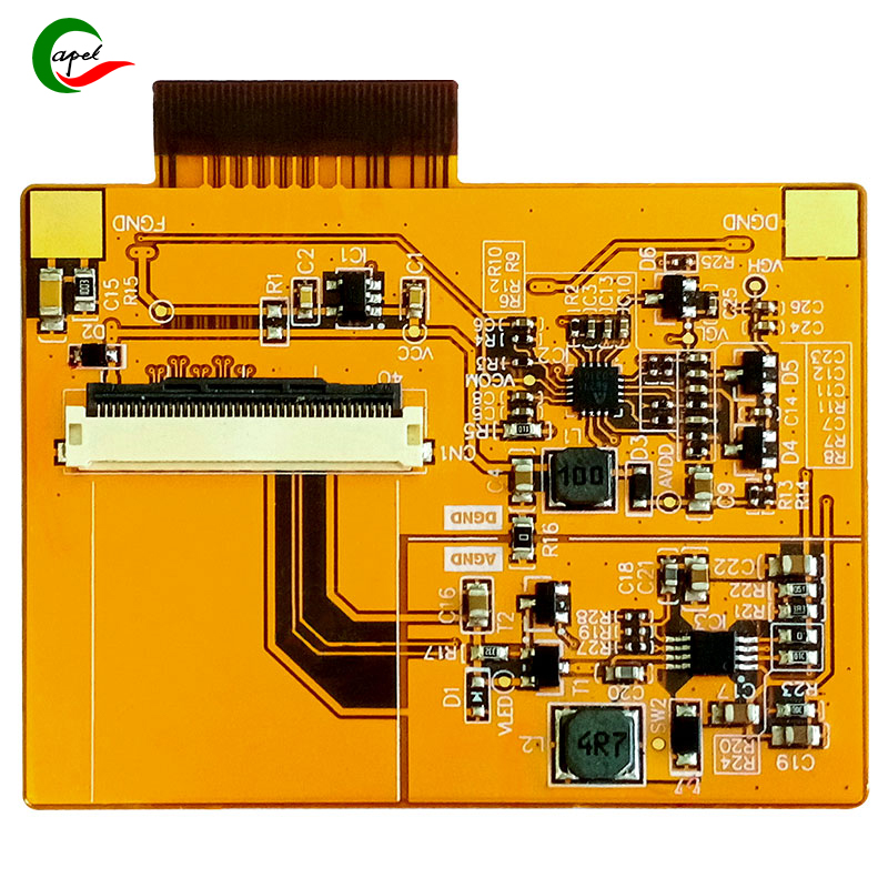
Capel supports rigid flex pcb with Min Line Space/ width 0.035mm/0.035mm.Shenzhen Capel Technology Co., Ltd.established its own rigid flex pcb factory in 2009 and it is a professional Flex Rigid Pcb Manufacturer. With 15 years of rich project experience, rigorous process flow, excellent technical capabilities, advanced automation equipment,comprehensive quality control system, and Capel has a professional experts team to provide global customers with high-precision, high-quality 1-32 layer rigid flex board, hdi Rigid Flex Pcb, Rigid Flex Pcb Fabrication, rigid-flex pcb assembly,fast turn rigid flex pcb,quick turn pcb prototypes.Our responsive pre-sales and after-sales technical services and timely delivery enable our clients to quickly seize market opportunities for their projects.
Post time: Aug-29-2023
Back


