
How to effectively manage conflicts between internal wires and external pad connections on multi-layer printed circuit boards?
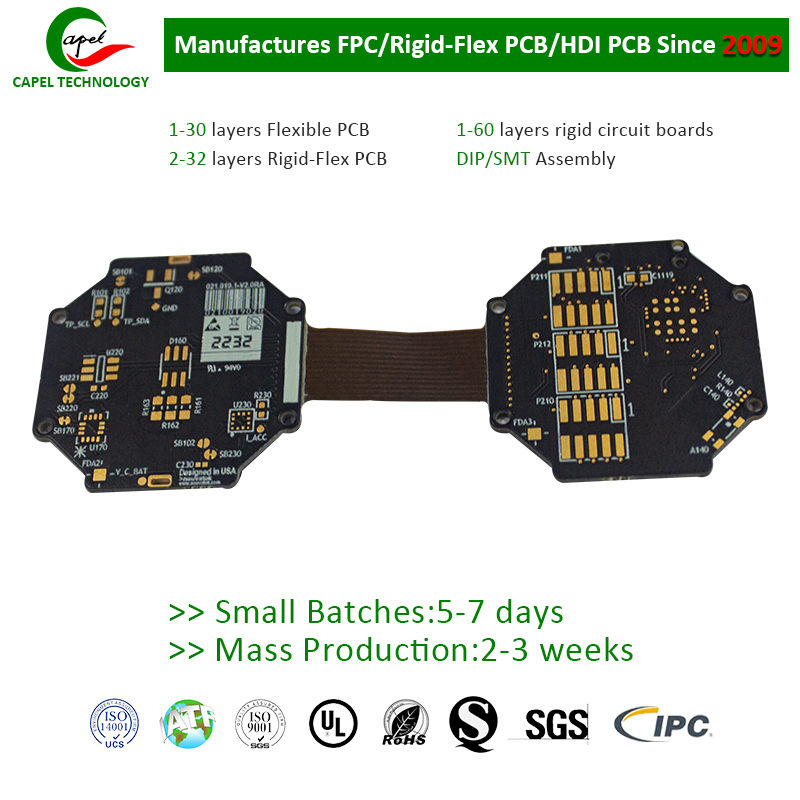
In the world of electronics, printed circuit boards (PCBs) are the lifeline that connects various components together, allowing for seamless communication and functionality. Multilayer PCBs, in particular, are becoming increasingly popular due to their enhanced functionality and higher component density. However, their complexity creates the challenge of managing conflicts between internal lines and external pad connections. In this blog, we will explore effective strategies to handle this conflict and ensure optimal performance and reliability.
1. Understand the conflict:
To effectively solve any problem, it is crucial to understand its root cause. Conflicts between internal lines and external pad connections arise due to their different requirements. Internal traces require smaller widths and spacing for high-density routing, while external pads require larger sizes for component soldering and physical connections. Conflicts between these requirements can lead to a variety of problems, such as loss of signal integrity, excessive heat generation, and even electrical shorts. Recognizing and understanding this conflict is the first step in finding a solution.
2. Optimize design:
The key to managing conflicts lies in optimizing the design of multi-layer PCBs. This can be achieved through the following strategies:
- Careful stackup planning: A well thought out stackup is critical to balancing the needs of internal traces and external pads. Placing internal signal layers closer to the midplane of the PCB stackup allows for controlled impedance and better signal integrity. On the other hand, placing the external pads on the outer layer provides better accessibility to the component.
- Proper wiring techniques: Utilize wiring techniques such as microvias and blind vias to connect internal lines to external pads. The smaller microvia diameter provides high routing density without compromising signal quality. Blind vias connect only a few adjacent layers, giving internal traces a direct path to external pads without having to traverse the entire PCB stack.
- Impedance matching considerations: Impedance mismatch between internal lines and external pads may cause signal reflections and performance degradation. Employ impedance matching techniques such as controlled dielectric constant, optimized trace widths, and proper termination to ensure consistent signals across the entire PCB.
- Thermal Management: Adequate cooling is critical for reliable PCB operation. Design PCBs with thermal vias to efficiently transfer heat generated by components located near external pads to the inner layers.
3. Collaboration and communication:
Managing conflicts in PCB design often requires collaboration between different stakeholders, such as design engineers, PCB manufacturers, and assembly experts. Maintaining effective communication channels is critical to ensuring everyone understands design constraints and requirements. Regular meetings and discussions can help align expectations and resolve conflicts through shared problem-solving.
4. Simulation and analysis:
Use simulation and analysis tools to verify your design’s electrical performance, signal integrity, and thermal characteristics. These tools provide a comprehensive understanding of PCB behavior, helping to identify potential conflicts and fine-tune designs before manufacturing. Simulation also helps optimize signal routing and ensure impedance matching between internal lines and external pads.
5. Prototyping and testing:
Prototyping and testing are important steps to verify design functionality and resolve any remaining conflicts. By closely monitoring the PCB during testing, engineers can identify areas where conflicts persist and further refine the design. Prototyping also provides the opportunity to validate thermal management techniques and ensure overall PCB reliability.
In summary
Managing conflicts between internal traces and external pad connections in multilayer PCBs requires a holistic approach that combines optimized design practices, effective communication, simulation and analysis tools, and thorough testing. By understanding the root causes of conflicts and implementing the strategies discussed, you can achieve a balanced design that ensures the overall performance, reliability, and functionality of your multilayer PCB.
Post time: Sep-26-2023
Back


