
Neglecting the construction quality of a board can lead to various problems during PCB development. These can include manufacturing difficulties, low yields, and even premature failure in real-world applications. However, there are some effective design strategies to mitigate these troublesome and expensive surprises. So, let’s first address your question: “What exactly is the PCB Fabrication process?” and then dive into the importance of understanding this process for successful PCB development.
Wondering how to turn your great idea into a tangible printed circuit board (PCB)? Well, take it easy, let’s not rush into the making process just yet. Understanding the basic connections and steps that link a schematic or concept to the actual creation of a PCB is critical. By taking the time to delve into the intricate web of terms and their interdependencies, we can pave the way for a smoother PCB manufacturing journey.
Introduction to PCB Development:
Wondering how to bring innovative circuit board designs to life? This is where PCB development comes in! It’s an exciting process to take your design from concept to production while ensuring top-notch quality. Through the three key stages of design, manufacturing and testing, we spare no effort to deliver superior results. Plus, get ready for an iterative journey as we fine-tune and refine your designs in the allotted development time to create the ultimate masterpiece. Get ready to watch your vision become an extraordinary reality!
Introduction to PCB Manufacturing:
Ready to turn your circuit board design dreams into reality? PCB fabrication is an integral process in turning your blueprints into tangible reality. It’s a dynamic two-step journey that begins with board fabrication, where cutting-edge technologies meticulously shape and shape your design. From there, watch in awe as we transition seamlessly into the exciting world of printed circuit board assembly (PCBA). Our skilled specialists perfectly incorporate complex components, ensuring optimum performance and functionality. With us by your side, your board vision will flourish and exceed expectations, paving the way for unparalleled success. Get ready to revolutionize the world with your innovations!
Get ready for PCB Testing:
Are you close to finishing your state-of-the-art circuit board? Now is the time to unleash the true potential of PCB testing through its power. As a critical third stage in the PCB development process, testing (also known as provisioning) takes place immediately after fabrication. This critical stage is designed to assess whether your board is capable of flawlessly executing its intended operational mandate. No expense was spared in our meticulous testing program, highlighting any glitches or areas in need of enhanced performance. Armed with this valuable information, we start another cycle to quickly incorporate design changes to push your board to peak performance. Experience the thrill of perfection when your vision becomes reality!
Experience the Power of PCB Assembly:
Taking your circuit board from concept to reality has never been easier with our advanced PCB assembly services. As a key element in the PCB manufacturing process, PCBA paves the way for seamless integration of circuit board components onto bare boards. Through precise welding processes, our expert technicians transform your design into a fully functional masterpiece. Whether you need Surface Mount Technology (SMT) or Through Hole Technology (THT), our state-of-the-art assembly technology ensures impeccable precision and flawless execution. Trust us to bring your vision to life and witness our unparalleled quality of PCB assembly services.
Exploring the PCB Manufacturing Process:
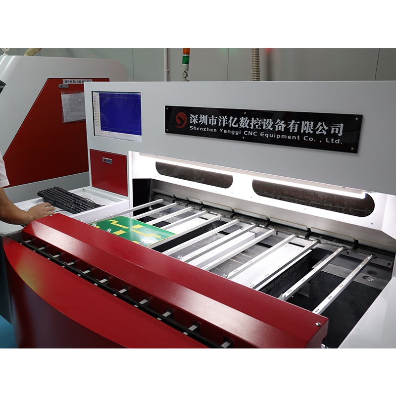
Ever wondered how your board design came to be? Our advanced PCB manufacturing process will ensure your vision becomes a reality. This step-by-step process takes your design package and transforms it into a physical structure that matches your tee’s specifications. We combine innovative technology with meticulous attention to detail to give your boards a new look. From creating the board layout to etching, drilling, and finally finishing touches, our expert team ensures that every step is executed flawlessly. Experience our precision and excellence in PCB manufacturing and watch your designs come to life right before your eyes.
Visualize your ideal design on Copper Clad Laminate:
Imagine your perfect circuit board layout implemented on top quality Copper Clad Laminate. With our state-of-the-art imaging technology, we enable you to see your design take shape and ensure that every detail is executed with precision.
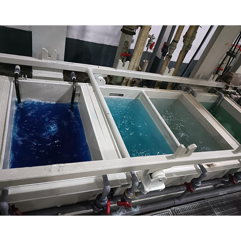
Professionally remove excess copper to expose traces and pads:
Our skilled technicians go the extra mile to etch or remove any excess copper from the inner layers of the PCB. In doing so, we reveal the complex traces and pads that are critical to the smooth operation of electronic circuits.
Precisely Fabricate Robust PCB Layer Stackups:
Our experienced professionals take your PCB layer stackups to the next level by expertly laminating circuit board materials together. Through carefully controlled heating and pressing processes, we ensure safe and reliable bonding at high temperatures. You can trust your boards to withstand the harshest conditions.
Drilling holes for secure mounting and connections:
We understand the importance of secure mounting and perfect connections. Our advanced drilling techniques allow us to create precise holes for mounting components, through-hole pins and vias, ensuring seamless integration of the PCB into the final product.
Exposing hidden traces and pads on the surface:
We continue to take a meticulous approach when we etch or remove any excess copper from the surface layers of the board. By doing this, we reveal the well-designed traces and pads that allow your circuits to flourish.
Reinforced pinholes and vias for maximum performance:
Your board performance is our top priority. Using our state-of-the-art plating technology, we reinforce pinholes and vias to maximize conductivity and ensure long-lasting reliability.
Protect your PCB with a protective coating or solder mask:
We pride ourselves on providing an extra layer of defense for your board. Our team applies a protective coating or solder mask to the surface to extend the life of the PCB and protect it from environmental elements.
Personalize your board with screen printing:
your brand image matters. That’s why we offer customizable screen printing options for your PCBs. Add reference and polarity indicators, logos, or any other markings to differentiate your product from those of your competitors.
Optimize your PCB appearance with optional copper finishes:
We firmly believe that with a little more effort, your expectations can be exceeded. For added aesthetics, we offer the option to add a copper finish to specific areas of the board surface to ensure a polished and professional look.
Now, let’s dive into what this all means for PCB development:
As you dive into the world of PCB development, our comprehensive manufacturing process ensures that your designs come out exactly as you envisioned them. From imaging and etching to drilling, plating and adding protective coatings, each step is meticulously executed with precision and expertise. Experience the difference in our PCB manufacturing process and watch your designs flourish into high-performance boards.
Uncovering the Power of Understanding PCB Manufacturing Inside and Out:
Consider the importance of gaining a deep understanding of the PCB manufacturing process. While PCB fabrication itself may not involve design, it is a key outsourced activity that is handled by experienced contract manufacturers (CMs). While manufacturing itself is not a design task, it is carefully executed according to the exact specifications you provide to the CM.
Unlock the Secrets Behind Optimal PCB Implementation: Imagine the possibility of witnessing the perfect circuit board blueprint brought to life using state-of-the-art manufacturing techniques. With our expertise in cutting-edge imaging technology, we enable you to witness every detail of your design take shape with absolute precision.
Let the masters clear the way by removing excess copper:
Our skilled technicians go above and beyond by expertly etching or removing any unwanted copper residue from the inner layers of the PCB. This process reveals complex traces and pads that are critical to the seamless operation of electronic circuits.
Take Your PCB Layer Stack Up to New Heights:
With our experienced professionals at the helm, we take your PCB layer stack up to the next level by meticulously laminating circuit board materials together. Through careful heating and pressing, we ensure a safe and reliable bond even under the most demanding conditions.
Drilling Precision Holes for Rock-Solid Mounting and Connections:
We understand the critical importance of secure mounting and flawless connections. That’s why our advanced drilling techniques allow us to form precise holes for component mounting, through-hole pins and vias. Rest assured that your PCB will integrate seamlessly into your final product.
Hidden treasures are brought to light through delicate surface etching:
our attention to detail remains the same. With careful touch, we can expertly etch or remove excess copper on the surface layer of the board. By doing this, we introduce well-designed traces and pads that power the success of your circuit. Reinforced pinholes and vias for resilient performance: When it comes to board performance, we don’t compromise. Utilizing state-of-the-art plating techniques, we reinforce your pinholes and vias, maximizing electrical conductivity and ensuring unrivaled durability.
Protect your PCB with a protective coating or solder mask:
As staunch protectors of circuit boards, we apply a protective coating or solder mask to protect its delicate components from environmental elements. Trust us to extend its lifespan.
Unleash your brand identity with unique screen printing:
your brand deserves to shine. That’s why customization is at the heart of our services. Choose from our customizable screen printing options and add reference designators, logos or any other markings to make your products unique.
Enhance aesthetics with an optional copper finish:
We believe excellence is in the details. To enhance the appearance of the board, we offer an optional copper finish on specific areas of the surface, ensuring a refined and totally professional look.
Now, let’s dive into the world of PCB development:
Embark on an extraordinary journey as we bring your design to life through our comprehensive manufacturing process. From imaging and etching to drilling, plating and protective coating, every stage exudes craftsmanship and precision. Embrace the difference our PCB manufacturing process makes and watch your creations blossom into extraordinary high-performance boards.
Uncover the untapped potential of seamless collaboration:
Imagine perfect harmony between your design vision and the expertise of your contract manufacturer (CM). We understand that in most cases your CM may not have access to your design intent or performance goals. This knowledge gap can hinder the decision-making process and can affect critical aspects such as material selection, layout, via placement and pattern, trace parameters, and other factors that significantly affect manufacturability, production yield, and post-deployment performance. your PCB.
Bridging the Gap Through Informed Manufacturing Choices:
At Shenzhen Capel Technology Co., Ltd, we believe that seamless collaboration is the key to unlocking the true potential of PCBs. Our dedicated team works closely with you to understand your performance goals, bridging the gap between your design intent and manufacturing decisions. Armed with this invaluable insight, we ensure that every choice we make, whether it’s material selection, layout optimization, precise via placement or trace parameter tuning, is perfectly aligned with your goals.
Maximize PCB performance with expert manufacturing insight:
Having an experienced partner who understands the complexities of PCB manufacturing can make all the difference. Drawing on our in-depth knowledge of manufacturing processes and their impact on PCBs, we strive to optimize every aspect of the manufacturing process. From selecting the ideal material to fine-tuning layout and routing parameters, we relentlessly seek to maximize the manufacturability, production yield and long-term performance of our PCBs.
Provide your CM with design intent and performance goals:
Collaboration is key, and we believe in providing your CM with critical insight into your design intent and performance expectations. We remove any uncertainty that may arise during the manufacturing process by ensuring that your CM fully understands your selection of materials, layout, via location and style, trace parameters, and other critical factors. This transparency not only improves PCB manufacturability, but also improves production yield and guarantees best-in-class performance after PCB deployment.
Unlock the Full Potential of Your PCB:
With Shenzhen Capel Technology Co., Ltd. by your side, you can rest assured that every step of the manufacturing process will meet your design intent and performance goals. Together we can harness the power of collaboration to manufacture PCBs that not only meet but exceed your expectations. Don’t let any uncertainty hold you back – join us to revolutionize your PCB manufacturing journey and witness the incredible results of an informative, harmonious partnership.
Unlock Hidden Potential:
Discover the power of seamless collaboration between you and your contract manufacturer (CM). We understand that your CM often lacks insight into your design intent and performance goals. This limitation can hinder the decision-making process and can affect critical aspects such as material selection, layout optimization, VIA positioning, trace parameters, and other factors that affect PCB manufacturability, production yield, and post-deployment performance.
Optimizing Manufacturability Through Smart Design Choices:
At Shenzhen Capel Technology Co., Ltd., we believe that unlocking the true potential of a PCB begins with smart design choices. For optimal manufacturability, we focus on key factors such as maintaining proper clearance between surface elements and board edges. In addition, we carefully select materials with high coefficient of thermal expansion (CTE) to withstand PCBAs, especially lead-free soldering. These careful decisions can prevent redesign problems and keep the manufacturing process running smoothly. Additionally, if you decide to panelize your design, we ensure that every step of the way is well thought out.
Accurately improve board yield:
Successful manufacturing does not necessarily mean a compromise in quality. Even with manufacturing challenges, we have the expertise to deliver high yields on your boards. For example, by avoiding design parameters that are outside the tolerance range of the CM device, we can minimize the chances of a board being unusable. With our innovative manufacturing practices, you can confidently expect high-quality PCBs that meet your performance goals.
Ensuring Reliability for Every Application:
A PCB’s success depends largely on its classification according to IPC-6011. For rigid PCBs, three different classification levels exist, setting specific construction parameters for superior performance reliability. Our meticulous approach ensures that your board meets or exceeds the classification required for your intended use. By avoiding the pitfalls of lower classified building panels, we can prevent inconsistent handling or premature failure of the panels. Trust Shenzhen Capel Technology Co., Ltd. for consistent and reliable performance.
Enhance Your PCB Journey:
Shenzhen Capel Technology Co., Ltd. As your trusted partner, we follow a strict PCB manufacturing process and we ‘ll help you realize your PCB’s full potential. We work collaboratively to ensure your CM fully understands your design intent and performance goals. By bridging the gap between your vision and manufacturing decisions, we pave the way for seamless execution, optimized manufacturability, higher yields and unwavering reliability. Don’t let miscommunication hold you back from success – revolutionize your PCB journey with us and experience the transformative results of a truly aligned partnership.
Post time: Sep-06-2023
Back


