
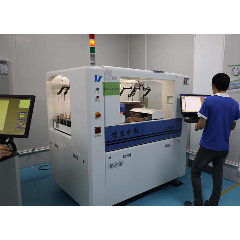
High frequency applications require meticulous attention to detail and precise manufacturing processes. When it comes to PCB prototyping for such applications, specific requirements must be met to ensure optimal performance and reliability. Capel has 15 years of experience in circuit board projects and has developed extensive expertise in PCB prototyping for high frequency applications. Our professional technical R&D team is committed to providing fast and reliable PCB prototype manufacturing for customers in the high-frequency application industry. From procurement to production and testing, we provide one-stop reliable solutions.
Before we delve into the specific requirements for PCB prototyping in high-frequency applications, let’s first understand what accurate and efficient prototyping means in this field. High-frequency applications include industries as diverse as telecommunications, aerospace, medical equipment, and wireless systems. In these industries, higher frequency signal transmission and reception are critical.
PCB prototyping for high-frequency applications requires careful consideration of several key factors to ensure optimal signal integrity, minimal losses, and reduced interference. Let’s explore some of the requirements in detail:
1. Material selection: Choosing the right PCB material is crucial for high-frequency applications. Dielectric constant (Dk), dissipation factor (Df) and thermal conductivity are key factors to consider. Materials such as PTFE or PTFE laminates have excellent electrical properties and low signal loss at high frequencies.
2. Stackup design: Proper stackup design is critical to achieving controlled impedance. Maintaining consistent dielectric thickness and copper plating thickness is critical to signal integrity. Controlled impedance helps minimize signal reflections and losses, ensuring reliable data transmission.
3. Controlled impedance: Impedance matching is critical for high-speed digital signals and RF circuits. Signals with different impedances can cause signal reflections, signal attenuation, and overall performance degradation. For high frequency applications, precise impedance control of the entire PCB is necessary.
4. Ground and power layers: Effective grounding techniques play a vital role in high-frequency design. A consistent dedicated ground plane provides a low-impedance return path for current flow, minimizing signal interference and crosstalk. Proper power plane distribution helps provide clean, stable power throughout the board.
5. RF Shielding: To prevent electromagnetic interference (EMI) and radio frequency interference (RFI), it is critical to use appropriate RF shielding technology. Copper shielding, RF shielding cans, and strategic placement of components can significantly reduce the effects of external interference and improve signal quality.
6. Component placement and routing: Component placement and routing must be carefully considered to minimize lead length and signal interference. Shorter traces reduce signal propagation time, thereby reducing the chance of signal degradation. Proper ground separation and noise isolation are also critical.
7. Signal trace crossings: In high-frequency applications, signal trace crossings should be avoided or carefully planned to minimize any adverse impact on signal integrity. Proper spacing and isolation techniques help reduce signal distortion and crosstalk.
8. Testing and Validation: Rigorous testing and validation procedures are critical to ensure the reliability and functionality of high-frequency PCB prototypes. Advanced test techniques, such as time domain reflectometry (TDR), can help evaluate performance and diagnose any signal integrity issues.
At Capel, we understand the importance of these specific requirements for PCB prototyping in high frequency applications. With our 15 years of experience and professional technical R&D team, we have mastered the art of producing reliable and efficient PCB prototypes. Our one-stop reliable solutions include procurement, production and testing, guaranteeing customer satisfaction.
In summary, PCB prototyping for high-frequency applications requires attention to detail and compliance with specific requirements. Materials, stackup design, impedance control, grounding techniques, RF shielding, component layout and test procedures all play a vital role in ensuring optimal performance. Capel’s expertise in PCB prototype production for high frequency applications makes us an ideal partner for companies in the high frequency application industry. Trust us to deliver fast, reliable PCB prototypes that meet your specific requirements and exceed your expectations.
Post time: Oct-16-2023
Back


