
Design considerations for multilayer flexible PCBs play a vital role in ensuring the reliability and functionality of electronic devices. As technology continues to evolve, the demand for flexible PCBs is growing rapidly due to their numerous advantages in terms of size reduction, weight reduction, and increased versatility. However, designing a multilayer flexible PCB requires careful consideration of various factors to ensure optimal performance. In this blog post, we explore key design considerations for multilayer flexible PCBs and discuss the challenges associated with their design and manufacturing process.
One of the main design considerations for multilayer flex PCBs is the choice of substrate material. Flexible PCBs rely on flexible substrate materials such as polyimide (PI) or polyester (PET) to provide the necessary flexibility and durability. The choice of substrate material depends on specific application requirements, including temperature resistance, mechanical strength, and reliability. Different substrate materials have different levels of thermal stability, dimensional stability, and bend radii, and these must be carefully evaluated to ensure that the PCB can withstand the operating conditions it will face.
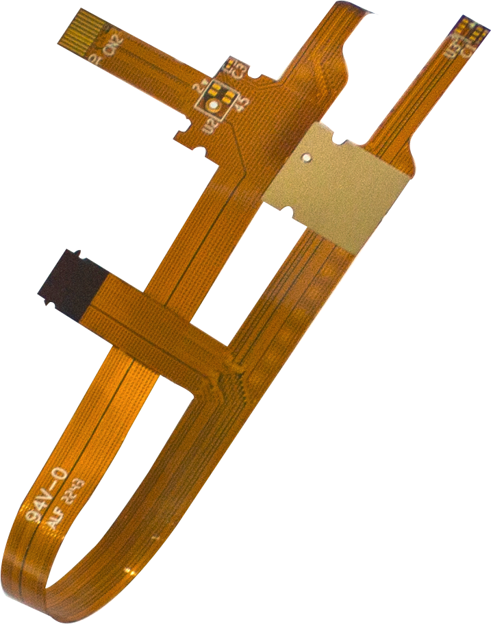
Another important consideration is the stackup design of the multilayer flexible PCB. Stackup design refers to the arrangement of multiple layers of conductive traces and dielectric material within a PCB. Careful planning of layer order, signal routing, and power/ground plane placement is critical to ensure optimal signal integrity, electromagnetic compatibility (EMC), and thermal management. The stack-up design should minimize signal crosstalk, impedance mismatch, and electromagnetic interference (EMI) to guarantee reliable and robust performance of electronic devices.
The routing of signal and power/ground planes presents additional challenges in multilayer flex PCBs compared to traditional rigid PCBs. The flexibility of the substrate allows complex three-dimensional (3D) wiring, which can significantly reduce the size and weight of the final electronic device. However, it also creates difficulties in managing signal propagation delays, electromagnetic emissions, and power distribution. Designers must carefully plan routing paths, ensure proper signal termination, and optimize power/ground plane distribution to minimize noise and ensure accurate signal transfer.
Component placement is another important aspect of multilayer flex PCB design. Component layout must consider factors such as space constraints, thermal management, signal integrity, and assembly process. Strategically placed components help minimize signal path length, reduce signal transmission delays, and optimize thermal dissipation. Component size, orientation and thermal characteristics must be considered to ensure efficient heat dissipation and prevent overheating in dense multilayer structures.
In addition, the design considerations for multilayer flexible PCBs also extend to the manufacturing process. Flexible substrate materials, delicate conductive traces, and complex wiring patterns require specialized manufacturing techniques. Designers must work closely with manufacturers to ensure design specifications are compatible with the manufacturing process. They must also consider potential manufacturing constraints, such as minimum trace width, minimum hole size and tolerance requirements, to avoid design flaws that could affect the overall performance and reliability of the PCB.
The design considerations discussed above highlight the complexity of designing a multilayer flexible PCB. They emphasize the importance of a holistic and systems approach to PCB design, where factors such as substrate material selection, stackup design, routing optimization, component placement, and manufacturing process compatibility are carefully evaluated. By incorporating these considerations into the design phase, designers can create multilayer flexible PCBs that meet the stringent requirements of modern electronic devices.
In summary, design considerations for multilayer flexible PCBs are critical to ensuring the reliability, functionality, and performance of electronic devices. Substrate material selection, stackup design, routing optimization, component placement, and manufacturing process compatibility are key factors that must be carefully evaluated during the design phase. By considering these factors, designers can create multilayer flexible PCBs that offer the benefits of reduced size, reduced weight, and increased versatility, while still meeting the stringent requirements of modern electronic applications.
Post time: Sep-02-2023
Back


