
Date: 2025-07-17
In today’s fast-paced digital world, the demand for smaller, lighter and more powerful electronic devices continues to grow. To meet these requirements, electronics manufacturers have introduced high-density interconnect (HDI) flexible PCB technology. Compared to traditional flex PCBs, HDI flex PCBs offer greater design flexibility, improved functionality, and enhanced reliability. In this article, we’ll explore what HDI flex PCBs are, their benefits, and how they differ from traditional flex PCBs.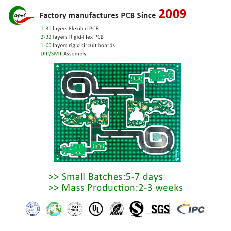
HDI flexible PCB, also known as high-density interconnect flexible printed circuit board, is a flexible circuit board that provides high circuit density and allows complex and
miniaturized designs. It combines the benefits of flexible PCBs, known for their ability to bend and adapt to different shapes, with high-density interconnect technology to
route more circuit traces in a compact space.
1.2 How is HDI flexible PCB made?
The manufacturing process of HDI flexible PCB involves several key steps:
Design:
The first step is to design the circuit layout, considering the size, shape and arrangement of the components and the desired function.
Material preparation:
Select and prepare the materials required for flexible PCBs, such as copper foil, adhesives, and flexible substrate materials.
Layer stacking:
Multiple layers of flexible material, copper foil, and adhesives are stacked together to form the basis of a circuit. Laser Drilling: Laser drilling is used to create small holes or vias that connect different layers of a circuit. This allows wiring in tight spaces.
Copper Plating:
Holes formed by laser drilling are plated with copper to ensure electrical connection between the different layers.
Circuit Etching:
Unnecessary copper is etched away, leaving traces of the desired circuit.
Solder Mask Application:
Solder mask is used to protect circuits and prevent short circuits during assembly.
Component Mounting:
Components such as integrated circuits, resistors, and capacitors are mounted on the flexible PCB using surface mount technology (SMT) or other suitable methods.
Tested and inspected:
Finished HDI flex PCBs are thoroughly tested and inspected to ensure proper functionality and quality.
1.3 Advantages of HDI flexible PCB:
Advantages of HDI flexible PCB Compared with traditional flexible PCB, HDI flexible PCB has several advantages, including:
Increased circuit density:
HDI technology enables higher density circuit trace routing, enabling more components to be placed in a smaller footprint. This results in a miniaturized and compact design.
Improved signal integrity:
Shorter routing distances in HDI flex PCBs result in less electromagnetic interference (EMI), resulting in better signal integrity, minimizing signal distortion and ensuring reliable performance.
Enhanced Reliability:
Compared to traditional flex PCBs, HDI flex PCBs have fewer stress points and are better resistant to vibration, bending, and thermal stress. This improves the overall reliability and lifetime of the circuit.
Design flexibility:
HDI technology enables complex circuit designs, allowing the combination of multiple layers, blind and buried vias, fine-pitch components, and high-speed signal routing.
Cost savings:
Despite its complexity and miniaturization, HDI flex PCBs can save costs by reducing the overall size and weight of the final product, making them more cost-effective for applications where space and weight are critical.
2.1 Basic differences in structure:
The main difference between the basic structure of HDI flexible PCB and traditional flexible PCB lies in the circuit density and the use of interconnection technology.
Traditional flex PCBs typically consist of a single layer of flexible substrate material such as polyimide, with copper traces etched on the surface. These boards typically have limited circuit density due to the lack of multiple layers and complex interconnects.
On the other hand, HDI flexible PCB adopts high-density interconnection technology, which can route more circuit traces in a compact space. This is achieved by using multiple layers of flex material stacked together with copper traces and adhesives. HDI flexible PCBs usually use blind and buried vias, which are holes drilled through specific layers to connect circuit traces inside the board, thereby improving the overall routing capability.
Additionally, HDI flex PCBs can employ microvias, which are smaller holes that allow denser trace routing. The use of microvias and other advanced interconnect technologies can significantly increase circuit density compared to traditional flex PCBs.
2.2 Main progress of HDI flexible PCB:
HDI flex PCBs have undergone significant advancements and advancements over the years. Some of the major advances made in HDI flexible PCB technology include:
Miniaturization:
HDI technology enables the miniaturization of electronic devices by allowing more circuit traces to be routed in less space. This paves the way for the development of smaller, more compact products such as smartphones, wearable devices and medical implants.
Increased circuit density:
Compared with traditional flexible PCBs, the use of multi-layers, blind buried vias, and microvias in HDI flexible PCBs significantly increases circuit density. This makes it possible to integrate more complex and advanced circuit designs in a smaller area.
Higher speed and signal integrity:
HDI flex PCBs can support high-speed signals and improve signal integrity as the distance between components and interconnects decreases. This makes them suitable for applications requiring reliable signal transmission, such as high-frequency communication systems or data-intensive equipment.
Fine-pitch component layout:
HDI technology facilitates the layout of fine-pitch components, which means components can be placed closer together, resulting in further miniaturization and densification of circuit layout. Fine-pitch component placement is critical for advanced applications requiring high-performance electronics.
Enhanced thermal management:
HDI flex PCBs have better thermal management capabilities due to the use of multiple layers and increased surface area for heat dissipation. This allows efficient handling and
cooling of high power components, ensuring their peak performance.
2.3 Function and performance comparison:
When comparing the functionality and performance of HDI flex PCBs to traditional flex PCBs, there are several factors to consider:
Circuit Density:
Compared to traditional flex PCBs, HDI flex PCBs offer significantly higher circuit density. HDI technology can integrate multi-layer, blind vias, buried vias, and microvias, enabling more complex and denser circuit designs.
Signal Integrity:
The reduced distance between traces and the use of advanced interconnection techniques in HDI flex PCBs improves signal integrity. This means better signal transmission and lower signal distortion compared to conventional flex PCBs.
Speed and Bandwidth:
HDI flex PCBs are able to support higher speed signals due to enhanced signal integrity and reduced electromagnetic interference. Conventional flex PCBs can have limitations in terms of signal transmission speed and bandwidth, especially in applications that require high data rates.
Design flexibility:
Compared with traditional flex PCBs, HDI flex PCBs provide greater design flexibility. The ability to incorporate multiple layers, blind and buried vias, and microvias allows for more complex circuit designs. This flexibility is especially important for applications that require a compact design or have specific space constraints.
Cost:
HDI flex PCBs tend to be more expensive than traditional flex PCBs due to the increased complexity and advanced interconnection techniques involved. However, the miniaturization and improved performance offered by HDI flex PCBs can often justify the added cost when the overall cost of the final product is considered.
2.4 Reliability and Durability Factors:
Reliability and durability are critical factors for any electronic device or system. Several factors come into play when comparing the reliability and durability of HDI flex PCBs to traditional flex PCBs:
Mechanical flexibility:
Both HDI and traditional flex PCBs offer mechanical flexibility, allowing them to adapt to different shapes and bend without breaking. However, HDI flex PCBs may have additional structural reinforcement, such as additional layers or ribs, to support increased circuit density. This reinforcement enhances the overall reliability and durability of the HDI flex PCB.
Anti-vibration and shock:
Compared with traditional flexible PCB, HDI flexible PCB can have better anti-vibration and shock ability. The use of blind, buried, and microvias in HDI boards helps distribute stress more evenly, reducing the possibility of component damage or circuit failure due to mechanical stress.
Thermal Management:
Compared with traditional flex PCB, HDI flex PCB has multiple layers and larger surface area, which can provide better thermal management. This improves heat dissipation and helps increase the overall reliability and lifespan of the electronics.
Lifespan:
Both HDI and traditional flex PCBs can have a long lifespan if properly designed and manufactured. However, the increased circuit density and advanced interconnection techniques used in HDI flex PCBs require careful consideration of factors such as thermal stress, material compatibility, and reliability testing to ensure long-term performance.
Environmental factors:
HDI flex PCBs, like traditional flex PCBs, need to be designed and manufactured to withstand environmental factors such as humidity, temperature changes, and exposure to chemicals. HDI flex PCBs may require additional protective coating or encapsulation to ensure resistance to environmental conditions.
HDI flex PCBs offer several advantages over traditional flex PCBs in terms of circuit density, signal integrity, design flexibility, and reliability. The use of advanced interconnection techniques and miniaturization techniques make HDI flex PCBs suitable for applications requiring high-performance electronics in a compact form factor. However, these advantages come at a higher cost and the specific requirements of the application should be carefully considered to determine the most suitable PCB technology.
HDI (High Density Interconnect) flex PCBs are gaining popularity in the electronics industry due to their numerous advantages over traditional flex PCBs.
3.1 Miniaturization and space optimization:
Miniaturization and space optimization: One of the main advantages of HDI flexible PCB is the miniaturization and space optimization of electronic equipment. The use of high-density interconnect technology allows more circuit traces to be routed in a compact space. This in turn facilitates the development of smaller, more compact electronics. HDI flex PCBs are commonly used in applications such as smartphones, tablets, wearables, and medical devices where space is limited and compact size is critical.
3.2 Improve signal integrity:
Improve signal integrity: Signal integrity is a critical factor in electronic equipment, especially in high-speed and high-frequency applications. HDI flex PCBs excel at delivering higher signal integrity due to the reduced distance between components and interconnects. Advanced interconnection technologies used in HDI flex PCBs, such as blind vias, buried vias, and microvias, can significantly reduce signal loss and electromagnetic interference. Improved signal integrity ensures reliable signal transmission and reduces the risk of data errors, making HDI flex PCBs suitable for applications involving high-speed data transmission and communication systems.
3.3 Enhanced power distribution:
Enhanced Power Distribution: Another advantage of HDI flex PCB is its ability to enhance power distribution. With the increasing complexity of electronic devices and the need for higher power requirements, HDI flex PCBs provide an excellent solution for efficient power distribution. Using multiple layers and advanced power routing techniques enables better board-wide power distribution, minimizing power loss and voltage drop. Enhanced power distribution enables reliable operation of power-hungry components and reduces the risk of overheating, ensuring safety and optimum performance.
3.4 Higher component density :
Higher component density: Compared with traditional flexible PCB, HDI flexible PCB can achieve higher component density. The use of multi-layer and advanced interconnection technologies allows the integration of more electronic components in a smaller space. HDI flex PCBs can accommodate complex and dense circuit designs, which is critical for advanced applications that require more functionality and performance without compromising board size. With higher component density, manufacturers can design and develop highly complex and feature-rich electronic products.
3.5 Improve heat dissipation:
Improved heat dissipation: Heat dissipation is a critical aspect of electronic device design, as excess heat can lead to performance degradation, component failure and even system damage. Compared with traditional flexible PCB, HDI flexible PCB has better heat dissipation performance. The use of multiple layers and increased surface area allows for better heat dissipation, effectively removing and dissipating the heat generated by power-hungry components. This ensures optimum performance and reliability of electronic devices, especially in applications where thermal management is critical.
HDI flex PCBs have several advantages that make them an excellent choice for modern electronics. Their ability to be miniaturized and space optimized makes them ideal for applications where compact size is critical. Improved signal integrity ensures reliable data transmission, while enhanced power distribution enables efficient powering of components. HDI flex PCB’s higher component density accommodates more functions and features, while improved heat dissipation ensures optimal performance and longevity of electronic devices. With these advantages, HDI flex PCBs have become a necessity in various industries such as consumer electronics, telecom, automotive, and medical equipment.
HDI flexible PCB has a wide range of applications in different industries. Their miniaturization capabilities, improved signal integrity, enhanced power distribution, higher component density, and improved heat dissipation make them ideal for consumer electronics, medical devices, the automotive industry, aerospace and defense systems, and the Internet of Things and wearables. important component in the device. HDI flex PCBs enable manufacturers to create compact, high-performance electronic devices to meet the growing demands of these industries.
4.1 Consumer Electronics:
HDI flexible PCB has a wide range of applications in the consumer electronics industry. With the continued demand for smaller, thinner, and more feature-rich devices, HDI flex PCBs enable manufacturers to meet these demands. They are used in smartphones, tablets, laptops, smart watches and other portable electronic devices. The miniaturization capabilities of HDI flexible PCBs allow the integration of multiple functions in a compact space, enabling the development of stylish and high-performance consumer electronics.
4.2 Medical devices:
The medical device industry relies heavily on HDI flex PCBs because of their reliability, flexibility, and small form factor. Electronic components in medical devices such as pacemakers, hearing aids, blood glucose monitors and imaging equipment require high precision. HDI flex PCBs can meet these requirements by providing high-density connections and improved signal integrity. Furthermore, their flexibility can be better integrated into wearable medical devices for patient comfort and convenience.
4.3 Auto Industry:
HDI flex PCBs have become an integral part of modern cars. The automotive industry requires high-performance electronics that can withstand challenging environments and deliver optimal functionality. HDI flex PCBs provide the necessary reliability, durability and space optimization for automotive applications. They are used in various automotive systems including infotainment systems, navigation systems, powertrain control modules and advanced driver assistance systems (ADAS). HDI flex PCBs can withstand temperature changes, vibration and mechanical stress, making them suitable for harsh automotive environments.
4.4 Aerospace and Defense:
The aerospace and defense industry requires highly reliable electronic systems that can withstand extreme conditions, vibration and high-speed data transmission. HDI flex PCBs are ideal for such applications because they provide high-density interconnects, improved signal integrity, and resistance to environmental factors. They are used in avionics systems, satellite communications, radar systems, military equipment and drones. The miniaturization capabilities of HDI flex PCBs help in the development of lightweight, compact electronic systems that enable better performance and more functionality.
4.5 IoT and Wearable Devices:
The Internet of Things (IoT) and wearable devices are transforming industries ranging from healthcare and fitness to home automation and industrial monitoring. HDI flex PCBs are key components in IoT and wearable devices due to their small form factor and high flexibility. They enable the seamless integration of sensors, wireless communication modules, and microcontrollers in devices such as smart watches, fitness trackers, smart home devices, and industrial sensors. The advanced interconnect technology in HDI flex PCBs ensures reliable data transmission, power distribution, and signal integrity, making them suitable for the demanding requirements of IoT and wearable devices.
Designing an HDI flex PCB requires careful consideration of layer stack-up, trace spacing, component placement, high-speed design techniques, and challenges associated with assembly and manufacturing. By effectively addressing these design considerations, Kaboer can develop high-performance HDI flex PCBs suitable for a variety of applications.
5.1 Layer stacking and routing:
HDI flex PCBs typically require multiple layers to achieve high-density interconnects. When designing the layer stack, factors such as signal integrity, power distribution, and thermal management must be considered. Careful layer stacking helps optimize signal routing and minimize crosstalk between traces. Routing should be planned to minimize signal skew and ensure proper impedance matching. Sufficient space must be allocated for vias and pads to facilitate interconnection between layers.
5.2 Trace Spacing and Impedance Control:
HDI flex PCBs usually have a high density of traces, maintaining proper trace spacing is critical to prevent signal interference and crosstalk. Designers must determine the proper trace width and spacing based on the desired impedance. Impedance control is critical to maintaining signal integrity, especially for high-speed signals. Designers should carefully calculate and control trace width, spacing, and dielectric constant to achieve the desired impedance value.
5.3 Component placement:
Proper component placement is critical to optimize the signal path, reduce noise and minimize the overall size of the HDI flex PCB. Components should be placed strategically to minimize signal trace length and optimize signal flow. High-speed components should be placed closer together to minimize signal propagation delays and reduce the risk of signal distortion. Designers should also consider thermal management aspects and ensure components are placed in a manner that allows heat dissipation.
5.4 High-speed design technology:
HDI flex PCBs typically cater to high-speed data transmission where signal integrity is critical. Proper high-speed design techniques, such as controlled impedance routing, differential pair routing, and matched trace lengths, are critical to minimizing signal attenuation. Signal integrity analysis tools can be used to simulate and verify the performance of high-speed designs.
5.5 Assembly and Manufacturing Challenges:
The assembly and manufacture of HDI flex PCBs presents several challenges. The flexible nature of PCBs requires careful handling during assembly to avoid damaging delicate traces and components. Accurate component placement and soldering may require specialized equipment and techniques. The fabrication process needs to ensure precise alignment of the layers and proper adhesion between them, which may involve additional steps such as laser drilling or laser direct imaging.
Additionally, the small size and high component density of HDI flex PCBs can pose challenges for inspection and testing. Special inspection techniques such as X-ray inspection may be required to detect defects or failures in PCBs. Furthermore, since HDI flex PCBs usually use advanced materials and technologies, the selection and qualification of suppliers is crucial to ensure the quality and reliability of the final product.
The future of HDI flexible PCB technology will be characterized by increasing integration and complexity, the adoption of advanced materials, and the expansion of IoT and wearable technologies. These trends will drive industries to develop smaller, more powerful, and multifunctional electronic devices.
6.1 Increased integration and complexity:
HDI flexible PCB technology will continue to develop in the direction of increasing integration and complexity. As electronic devices become more compact and feature-rich, there is a growing demand for HDI flex PCBs with higher circuit density and smaller form factors. This trend is driven by advances in manufacturing processes and design tools that enable finer-pitch traces, smaller vias, and tighter interconnect pitches. Integrating complex and diverse electronic components on a single flexible PCB will become more
common, reducing size, weight and overall system cost.
6.2 Using advanced materials:
In order to meet the needs of higher integration and performance, HDI flexible PCB will use advanced materials. New materials with enhanced electrical, thermal and mechanical properties will enable better signal integrity, improved heat dissipation and higher reliability. For example, the use of low-loss dielectric materials will allow higher frequency operation, while high thermal conductivity materials can enhance the thermal management capabilities of flex PCBs. Additionally, advances in conductive materials such as copper alloys and conductive polymers will enable higher current-carrying capabilities and better impedance control.
6.3 Expansion of IoT and Wearable Technology:
The expansion of the Internet of Things (IoT) and wearable technology will have a major impact on HDI flexible PCB technology. As the number of connected devices continues to grow, there will be an increasing need for flexible PCBs that can be integrated into smaller and more diverse form factors. HDI flex PCBs will play a vital role in the miniaturization of wearable devices such as smart watches, fitness trackers and healthcare sensors. These devices often require flexible PCBs to conform to the body and provide robust and reliable interconnectivity.
Moreover, the widespread adoption of IoT devices in various industries such as smart home, automotive, and industrial automation will drive the demand for HDI flexible PCBs with advanced features such as high-speed data transmission, low power consumption, and wireless connectivity. These advances will require PCBs to support complex signal routing, miniaturized components and integration with different sensors and actuators.
In summary, HDI flex PCBs have changed the electronics industry with their unique combination of flexibility and high-density interconnects. These PCBs offer many advantages over traditional flex PCBs, including miniaturization, space optimization, improved signal integrity, efficient power distribution, and the ability to accommodate high component densities. These properties make HDI flex PCBs suitable for use in a variety of industries, including consumer electronics, medical devices, automotive systems, and aerospace applications. However, it is important to consider the design considerations and manufacturing challenges associated with these advanced PCBs. Designers must carefully plan layout and routing to ensure optimal signal performance and thermal management. Furthermore, the manufacturing process of HDI flex PCBs requires advanced processes and techniques to achieve the required level of precision and reliability. Going forward, HDI flexible PCBs are expected to continue to evolve as technology advances. As electronic devices become smaller and more complex, the need for HDI flex PCBs with higher levels of integration and performance will only increase. This will drive further innovations and advancements in the field, leading to more efficient and versatile electronic devices across industries.
Shenzhen Kaboer Technology Co., Ltd. has been manufacturing flexible printed circuit boards (PCBs) since 2009. Currently, we are able to provide custom 1-30 layer flexible printed circuit boards. Our HDI (High Density Interconnect) flexible PCB manufacturing technology is very mature. Over the past 15 years, we have continuously innovated technology and accumulated rich experience in solving project-related problems for customers.
![]()
Kaboer manufacturing PCBs since 2009. Professional technology and high-precision Printed Circuit Boards involved in Medical, IOT, UAV, Aviation, Automotive, Aerospace, Industrial Control, Artificial Intelligence, Consumer Electronics etc..


 English


 Wechat
 +86 13670210335
 +86 13670210335
 E-mail