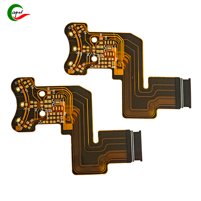
In this blog post, we will explore the key aspects of FPCB design and provide valuable insights into how to effectively design routing and component mounting.
Flexible printed circuit boards (FPCB) have revolutionized the electronics industry with their unparalleled flexibility and versatility. They offer many advantages over traditional rigid circuit boards, including smaller form factors, reduced weight and greater durability. However, when designing the wiring and component mounting of an FPCB, certain factors need to be carefully considered to ensure optimal performance and reliability.
1. Understand the unique characteristics of FPCB
Before we delve into the design process, it is important to understand the unique characteristics of FPCBs. Unlike rigid circuit boards, FPCBs are flexible and can be bent and twisted to fit a variety of form factors. Additionally, they consist of a thin layer of conductive material (usually copper) sandwiched between layers of flexible insulating material. These characteristics influence the design considerations and techniques used in cabling and component installation.
2. Plan the circuit layout
The first step in designing FPCB wiring and component mounting is to carefully plan the circuit layout. Position components, connectors, and traces to optimize signal integrity and minimize electrical noise. It is recommended to create schematics and simulate performance using specialized software before proceeding with the actual design.
3. Consider flexibility and bending radius
Since FPCBs are designed to be flexible, it is crucial to consider the bending radius during the design stage. Components and traces should be placed strategically to avoid stress concentrations that can lead to breakage or failure. It is recommended to maintain the minimum bending radius specified by the FPCB manufacturer to ensure the longevity of the circuit board.
4. Optimize signal integrity
Proper signal integrity is critical for reliable operation of FPCBs. To achieve this, signal interference, crosstalk and electromagnetic emissions must be minimized. Using a ground plane, shielding, and careful routing can significantly improve signal integrity. Additionally, high-speed signals should have controlled impedance traces to minimize signal attenuation.
5. Choose the right components
Choosing the right components for your FPCB design is critical to ensuring optimal performance and reliability. Consider factors such as size, weight, power consumption, and temperature range when selecting components. Additionally, components should be compatible with FPCB manufacturing processes such as surface mount technology (SMT) or through hole technology (THT).
6. Thermal management
As with any electronic system, thermal management is critical to FPCB design. FPCBs may generate heat during operation, especially when using power-intensive components. Ensure adequate cooling by utilizing heat sinks, thermal vias, or designing the board layout in a way that promotes efficient airflow. Thermal analysis and simulation can help identify potential hot spots and optimize the design accordingly.
7. Follow Design for Manufacturability (DFM) guidelines
To ensure a smooth transition from design to manufacturing, FPCB-specific design for manufacturing (DFM) guidelines must be followed. These guidelines address aspects such as minimum trace width, spacing, and annular rings to ensure manufacturability. Work closely with manufacturers during the design phase to resolve any potential issues and optimize designs for efficient production.
8. Prototype and test
After the initial design is completed, it is highly recommended to produce a prototype for testing and validation purposes. Testing should include functionality, signal integrity, thermal performance, and compatibility with intended use cases. Identify potential shortcomings or areas for improvement and iterate the design accordingly to achieve the desired performance.
In summary
Designing flexible printed circuit boards for routing and component mounting requires careful consideration of various factors unique to these flexible boards. An effective and robust FPCB design can be ensured by understanding the characteristics, planning the layout, optimizing signal integrity, selecting appropriate components, managing thermal aspects, following DFM guidelines, and performing thorough testing. Adopting these technologies will enable engineers to realize the full potential of FPCBs in creating innovative and cutting-edge electronic devices.
Post time: Sep-22-2023
Back


