
Introduction
Flexible printed circuit boards (FPCs) are revolutionizing the electronics industry, offering unparalleled flexibility and design possibilities. As the demand for more compact and lightweight electronic devices continues to grow, FPCs play a vital role in enabling innovative and flexible design solutions. Among the various types of FPCs, 2-layer flexible PCBs stand out for their versatility and applicability in a wide range of industries. In this comprehensive guide, we’ll explore the design and prototyping process of 2-layer flexible PCBs, focusing on their applications, materials, specifications, and surface finishes.
Product Type:2-Layer Flexible PCB
A 2-layer flex PCB, also known as a double-sided flex circuit, is a flexible printed circuit board consisting of two conductive layers separated by a flexible dielectric layer. This configuration provides designers with the flexibility to route traces on both sides of the substrate, allowing for greater design complexity and functionality. The ability to mount components on both sides of the board makes 2-layer flex PCBs ideal for applications requiring high component density and space constraints.
Applications
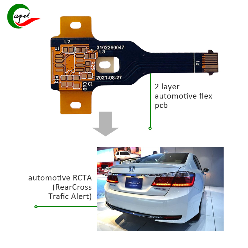
The versatility of 2-layer flex PCBs makes them suitable for a variety of applications in different industries. One of the prominent applications of 2-layer flexible PCB is in the field of automotive electronics. In the automotive industry, space and weight savings are key factors, and 2-layer flex PCBs offer the flexibility to meet these requirements. They are used in automotive control systems, sensors, lighting, infotainment systems, and more. The automotive industry relies on the durability and reliability of 2-layer flexible PCBs to ensure consistent performance in challenging environments.
In addition to automotive applications, 2-layer flexible PCBs are widely used in consumer electronics, medical devices, aerospace and industrial equipment. Their ability to adapt to irregular shapes, reduce weight and increase reliability makes them indispensable in a variety of electronic products.
Materials
2-Layer Flexible PCB Material selection is critical in determining the board’s performance, reliability, and manufacturability. The primary materials used to construct a 2-layer flexible PCB include polyimide (PI) film, copper, and adhesives. Polyimide is the substrate material of choice due to its excellent thermal stability, flexibility and high temperature resistance. Copper foil is used as the conductive material, which has excellent conductivity and solderability. Adhesive materials are used to bond the PCB layers together, ensuring mechanical stability and maintaining circuit integrity.
Line width, line spacing and board thickness
When designing a 2-layer flexible PCB, line width, line spacing and board thickness are key parameters, which directly affect the performance and manufacturability of the board. Typical line width and line spacing for 2-layer flexible PCBs are specified as 0.2mm/0.2mm, indicating the minimum width of conductive traces and the spacing between them. These dimensions are critical to ensure proper signal integrity, impedance control, and reliable soldering during assembly. Additionally, the board thickness of 0.2mm +/- 0.03mm plays an important role in determining the flexibility, bending radius and overall mechanical properties of a 2-layer flex PCB.
Minimum Hole Size and Surface Treatment
Achieving precise and consistent hole sizes is critical to 2-layer flexible PCB design, especially given the miniaturization trend of electronics. The specified minimum hole size of 0.1 mm demonstrates the ability of 2-layer flex PCBs to accommodate small and densely packed components. In addition, surface treatment plays a key role in improving the electrical performance and solderability of PCBs. Electroless Nickel Immersion Gold (ENIG) with a thickness of 2-3uin is a common choice for 2-layer flexible PCBs and offers excellent corrosion resistance, flatness, and solderability. ENIG surface treatments are particularly beneficial for enabling fine-pitch components and ensuring reliable solder joints.
Impedance and Tolerance
In high-speed digital and analog applications, impedance control is critical to maintaining signal integrity and minimizing signal distortion. Although no specific impedance values are provided, the ability to control the impedance of a 2-layer flex PCB is critical to meeting the performance requirements of electronic circuits. In addition, the tolerance is specified as ±0.1mm, which refers to the allowable dimensional deviation during the manufacturing process. Tight tolerance control is critical to ensuring accuracy and consistency in the final product, especially when dealing with micro-features and complex designs.
2 Layer Flexible PCB Prototyping Process
Prototyping is a critical stage in 2-layer flex PCB development, allowing designers to verify design, functionality, and performance before proceeding to full production. The prototyping process involves several key steps, including design verification, material selection, manufacturing, and testing. Design verification ensures that the board meets specified requirements and functionality, while material selection includes selecting the appropriate substrate, conductive materials and surface treatment based on application and performance criteria.
The fabrication of 2-layer flexible PCB prototypes involves the use of specialized equipment and processes to create the flexible substrate, apply conductive patterns, and assemble the components. Advanced manufacturing techniques such as laser drilling, selective plating and controlled impedance routing are used to achieve the required functionality and performance attributes. Once the prototype is manufactured, a rigorous testing and validation process is performed to evaluate electrical performance, mechanical flexibility and reliability under various environmental conditions. Feedback from the prototyping stage helps design optimization and improvements, ultimately resulting in a robust and reliable 2-layer flexible PCB design ready for mass production.
2 Layer Flexible PCB – FPC Design and Prototyping Process
Conclusion
In summary, 2-layer flex PCBs represent cutting-edge solutions for modern electronics design, offering unparalleled flexibility, reliability and performance. Its wide range of applications, advanced materials, precise specifications and prototyping processes make it an indispensable component in the electronics industry. As technology continues to evolve, 2-layer flexible PCBs will undoubtedly play a vital role in enabling innovative electronic products that meet the needs of today’s connected world. Whether in automotive, consumer electronics, medical devices or aerospace, the design and prototyping of 2-layer flexible PCBs is critical to driving the next wave of electronics innovation.
Post time: Feb-23-2024
Back


