
In this comprehensive article, we delve into the world of 4-layer PCB stackups, guiding you through best design techniques and considerations.
Introduction :
In the world of PCB (printed circuit board) design, achieving optimal stackup is critical to ensuring consistent performance and reliable functionality. To meet the ever-increasing demands of modern electronic equipment, such as faster speed, higher density, and reduced signal interference, a well-planned 4-layer PCB stackup is critical. This article serves as a comprehensive guide to help you understand the key aspects and considerations involved in achieving an optimal 4-layer PCB stack-up. So, let’s delve into the world of PCB stackup and uncover the secrets to a successful design!
content:
1. Understand the basics of 4-layer PCB stacking :
- PCB Stackup: What is it and why is it important?
- Key considerations for 4-layer stack design.
- The importance of proper layer arrangement.
- Signaling and distribution layers: roles and locations.
- Factors affecting the selection of inner core and prepreg materials.
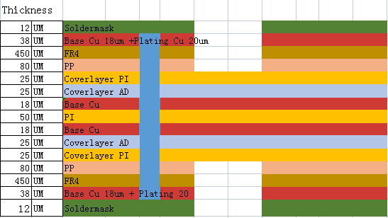
PCB stackup: PCB stackup refers to the arrangement and configuration of the different layers in a printed circuit board. It involves placing conductive, insulating, and signal distribution layers in a specific order to achieve the desired electrical performance and functionality of the PCB. PCB stackup is important because it determines the signal integrity, power distribution, thermal management and overall performance of the PCB.
Key Considerations for 4-Layer Stack Design:
When designing a 4-layer PCB stack-up, some key considerations include:
Signal integrity:
Placing signal layers close to each other while keeping power and ground planes adjacent improves signal integrity by reducing the impedance between signal traces and reference planes.
Power and Ground Distribution:
Proper distribution and placement of power and ground planes is critical for effective power distribution and noise reduction. It is important to pay attention to the thickness and spacing between the power and ground planes to minimize impedance.
Thermal management:
The placement of thermal vias and heat sinks and the distribution of thermal planes should be considered to ensure effective heat dissipation and prevent overheating.
Component placement and routability:
Careful consideration should be given to component placement and routing to ensure optimal signal routing and avoid signal interference.
The Importance of Proper Layer Arrangement: Layer arrangement in a PCB stack is critical to maintaining signal integrity, minimizing electromagnetic interference (EMI), and managing power distribution. Proper layer placement ensures controlled impedance, reduces crosstalk, and improves the overall performance of the PCB design.
Signal and distribution layers: Signals are typically routed on the top and bottom signal layers, while power and ground planes are on the inside. The distribution layer acts as a power and ground plane and provides a low impedance path for power and ground connections, minimizing voltage drop and EMI.
Factors Affecting Core and Prepreg Material Selection: The choice of core and prepreg materials for a PCB stackup depends on factors such as electrical performance requirements, thermal management considerations, manufacturability, and cost. Some important factors to consider include dielectric constant (Dk), dissipation factor (Df), glass transition temperature (Tg), thickness, and compatibility with manufacturing processes such as lamination and drilling. Careful selection of these materials ensures the desired electrical and mechanical properties of the PCB.
2. Techniques for optimal 4-layer PCB stackup:
- Careful component placement and trace routing for efficient power and signal integrity.
- The role of ground and power planes in minimizing noise and maximizing signal integrity.
- Determine the proper thickness and dielectric constant of each layer.
- Take advantage of controlled impedance routing for high-speed designs.
- Thermal considerations and thermal management in multilayer stacks.
These techniques help achieve an optimal 4-layer PCB stackup:
Careful component placement and trace routing: Efficient power and signal integrity can be achieved through careful component placement and trace routing. Group related components together and ensure short, direct connections between them. Minimize trace length and avoid crossing sensitive traces. Use proper spacing and keep sensitive signals away from noise sources.
Ground and Power Planes: Ground and power planes play a vital role in minimizing noise and maximizing signal integrity. Use dedicated ground and power planes to provide a stable reference plane and reduce electromagnetic interference (EMI). Ensure proper connections to these planes to maintain a low impedance path for return current.
Determine proper layer thickness and dielectric constant: The thickness and dielectric constant of each layer in the stack affects signal propagation and impedance control. Determine the desired impedance value and choose the appropriate thickness and dielectric constant for each layer accordingly. Review the PCB design guidelines and consider signal frequency and transmission line requirements.
Controlled Impedance Routing: Controlled impedance routing is critical for high-speed designs to minimize signal reflections, maintain signal integrity, and prevent data errors. Determine the required impedance values for critical signals and use controlled impedance routing techniques such as differential pair, stripline or microstrip routing, and controlled impedance vias.
Thermal Considerations and Management: Thermal management is critical to multilayer PCB stacks. Proper heat dissipation ensures components operate within their temperature limits and avoids potential damage. Consider adding thermal vias to transfer heat to internal ground planes or thermal pads, use thermal vias near high power components, and combine with heat sinks or copper pours for better heat distribution.
By implementing these techniques, you can ensure efficient power distribution, minimize noise, maintain signal integrity, and optimize thermal management in a 4-layer PCB stackup.
3. Design considerations for manufacturing 4-layer PCB :
- Balance manufacturability and design complexity.
- Design for Manufacturability (DFM) Best Practices.
- Via type and layout considerations.
- Design rules for spacing, trace width, and clearance.
- Work with PCB manufacturer to achieve optimal stackup.
Balancing Manufacturability and Design Complexity: When designing a 4-layer PCB, it is important to strike a balance between design complexity and manufacturing ease. Complex designs can increase manufacturing costs and potential errors. Simplifying designs by optimizing component placement, organizing signal routing, and using standardized design rules can improve manufacturability.
Design for Manufacturability (DFM) Best Practices: Incorporate DFM considerations into designs to ensure efficient and error-free manufacturing. This includes following industry-standard design rules, selecting appropriate materials and thicknesses, considering manufacturing constraints such as minimum trace width and spacing, and avoiding complex shapes or features that could add to manufacturing complexity.
Via Type and Layout Considerations: Selecting the proper via type and its layout is critical for a 4-layer PCB. Vias, blind vias, and buried vias each have their advantages and limitations. Carefully consider their use based on design complexity and density, and ensure proper clearance and spacing around vias to avoid signal interference and electrical coupling.
Design Rules for Spacing, Trace Width, and Clearance: Follow the recommended design rules for spacing, trace width, and clearance provided by the PCB manufacturer. These rules ensure that the design can be manufactured without any problems, such as electrical shorts or signal degradation. Maintaining adequate spacing between traces and components, maintaining proper clearance in high-voltage areas, and using the proper trace width for the desired current-carrying capacity are all important considerations.
Work with the PCB manufacturer for optimal stackup: Work with the PCB manufacturer to determine the optimal stackup for a 4-layer PCB. Factors to consider include copper layers, dielectric material selection and placement, desired impedance control, and signal integrity requirements. By working closely with manufacturers, you can ensure that PCB designs are aligned with their capabilities and manufacturing processes, resulting in more efficient and cost-effective production.
Overall, designing a 4-layer PCB requires a thorough understanding of manufacturability, adherence to DFM best practices, careful consideration of via type and layout, adherence to design rules, and collaboration with the PCB manufacturer to achieve an optimal stackup. By considering these factors, you can improve the manufacturability, reliability, and performance of your PCB design.
4. Advantages and limitations of 4-layer PCB stackup:
- Enhances signal integrity, reduces noise and minimizes EMI effects.
- Improved ability to implement high-speed designs.
- Space-saving advantage of compact electronics.
- Potential limitations and challenges of implementing a 4-layer stack.
Advantages of 4-layer PCB stackup:
Enhanced Signal Integrity:
Additional ground and power planes in the 4-layer stack help reduce signal noise and ensure better signal integrity for high-speed designs. The ground plane acts as a reliable reference plane, reducing signal crosstalk and improving impedance control.
Reduced noise and EMI impact:
The presence of ground and power planes in the 4-layer stack helps minimize electromagnetic interference (EMI) by providing shielding and improved signal grounding. This provides better noise reduction and ensures clearer signal transmission.
Increased ability to implement high-speed designs:
With additional layers, designers have more routing options. This enables complex high-speed designs with controlled impedance requirements, reducing signal attenuation and achieving reliable performance at higher frequencies.
Space-saving advantage:
4-layer stacking allows for a more compact and efficient design. It provides additional routing options and reduces the need for extensive interconnection between components, resulting in a smaller form factor for the overall electronic system. This is especially beneficial for portable electronics or densely populated PCBs.
Limitations and challenges of implementing a 4-layer stack:
Cost:
Implementing a 4-layer stackup increases the overall cost of the PCB compared to a 2-layer stackup. Cost is influenced by factors such as the number of layers, design complexity, and required manufacturing process. Additional layers require additional materials, more precise fabrication techniques, and advanced routing capabilities.
Design Complexity:
Designing a 4-layer PCB requires more careful planning than a 2-layer PCB. Additional layers present challenges in component placement, routing and via planning. Designers need to carefully consider signal integrity, impedance control, and power distribution, which can be more complex and time-consuming.
Manufacturing limitations:
Manufacturing 4-layer PCBs requires more advanced manufacturing processes and techniques. Manufacturers need to be able to accurately align and laminate layers, control the thickness of each layer, and ensure proper alignment of drilled and vias. Not all PCB manufacturers are capable of efficiently producing 4-layer boards.
Noise and Interference:
While a 4-layer stack-up helps reduce noise and EMI, insufficient design or layout techniques can still cause noise and interference issues. Improperly executed layer stacking or insufficient grounding can lead to unintentional coupling and signal attenuation. This requires careful planning and consideration of design layout and ground plane placement.
Thermal management:
The presence of additional layers affects heat dissipation and thermal management. Dense designs with limited space between layers can lead to increased thermal resistance and heat buildup. This requires careful consideration of component layout, thermal vias, and overall thermal design to avoid overheating issues.
It is important for designers to carefully evaluate their requirements, considering the advantages and limitations of a 4-layer PCB stackup, in order to make an informed decision on the best stackup for their particular design.
In summary, achieving an optimal 4-layer PCB stackup is critical to ensuring a reliable and high-performance electronic design. By understanding fundamentals, considering design techniques, and collaborating with PCB manufacturers, designers can take advantage of efficient power distribution, signal integrity, and reduced EMI effects. It must be remembered that a successful 4-layer stack design requires a careful approach and consideration of component placement, routing, thermal management and manufacturability. So take the knowledge provided in this guide and start your journey to achieve the best 4-layer PCB stack for your next project!
Post time: Aug-18-2023
Back


