
Introduction:
High-density interconnect (HDI) technology PCBs have revolutionized the electronics industry by enabling more functionality in smaller, lighter devices. These advanced PCBs are designed to enhance signal quality, reduce noise interference and promote miniaturization. In this blog post, we will explore the various manufacturing techniques used to produce PCBs for HDI technology. By understanding these complex processes, you will gain insight into the complex world of printed circuit board manufacturing and how it contributes to the advancement of modern technology.
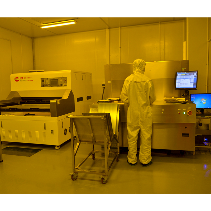
1. Laser Direct Imaging (LDI) :
Laser Direct Imaging (LDI) is a popular technology used to manufacture PCBs with HDI technology. It replaces traditional photolithography processes and provides more precise patterning capabilities. LDI uses a laser to directly expose photoresist without the need for a mask or stencil. This enables manufacturers to achieve smaller feature sizes, higher circuit density, and higher registration accuracy.
Additionally, LDI allows the creation of fine-pitch circuits, reducing the space between tracks and enhancing overall signal integrity. It also enables high-precision microvias, which are crucial for HDI technology PCBs. Microvias are used to connect different layers of a PCB, thereby increasing routing density and improving performance.
2. Sequential Building (SBU):
Sequential assembly (SBU) is another important manufacturing technology widely used in PCB production for HDI technology. SBU involves the layer-by-layer construction of the PCB, allowing for higher layer counts and smaller dimensions. The technology utilizes multiple stacked thin layers, each with its own interconnects and vias.
SBUs help integrate complex circuits into smaller form factors, making them ideal for compact electronic devices. The process involves applying an insulating dielectric layer and then creating the required circuitry through processes such as additive plating, etching and drilling. Vias are then formed by laser drilling, mechanical drilling or using a plasma process.
During the SBU process, the manufacturing team needs to maintain strict quality control to ensure optimal alignment and registration of the multiple layers. Laser drilling is often used to create small diameter microvias, thereby increasing the overall reliability and performance of HDI technology PCBs.
3. Hybrid manufacturing technology:
As technology continues to evolve, hybrid manufacturing technology has become the preferred solution for HDI technology PCBs. These technologies combine traditional and advanced processes to enhance flexibility, improve production efficiency and optimize resource utilization.
One hybrid approach is to combine LDI and SBU technologies to create highly sophisticated manufacturing processes. LDI is used for precise patterning and fine-pitch circuits, while SBU provides the necessary layer-by-layer construction and integration of complex circuits. This combination ensures successful production of high-density, high-performance PCBs.
In addition, the integration of 3D printing technology with traditional PCB manufacturing processes facilitates the production of complex shapes and cavity structures within HDI technology PCBs. This allows for better thermal management, reduced weight and improved mechanical stability.
Conclusion:
The manufacturing technology used in HDI Technology PCBs plays a vital role in driving innovation and creating advanced electronic devices. Laser direct imaging, sequential build and hybrid manufacturing technologies offer unique advantages that push the boundaries of miniaturization, signal integrity and circuit density. With the continuous advancement of technology, the development of new manufacturing technologies will further enhance the capabilities of HDI technology PCB and promote the continuous progress of the electronics industry.
Post time: Oct-05-2023
Back


