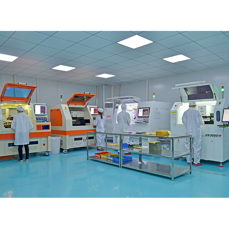
Rogers PCB, also known as Rogers Printed Circuit Board, is widely popular and used in various industries due to its superior performance and reliability. These PCBs are manufactured from a special material called Rogers laminate, which has unique electrical and mechanical properties. In this blog post, we’ll dive into the intricacies of Rogers PCB manufacturing, exploring the processes, materials, and considerations involved.
To understand the Rogers PCB manufacturing process, we must first understand what these boards are and grasp what Rogers laminates mean. PCBs are important components of electronic devices, providing mechanical support structures and electrical connections. Rogers PCBs are highly sought after in applications requiring high frequency signal transmission, low loss and stability. They are widely used in industries such as telecommunications, aerospace, medical and automotive.
Rogers Corporation, a renowned materials solutions provider, developed Rogers laminates specifically for use in manufacturing high-performance circuit boards. Rogers laminate is a composite material consisting of ceramic-filled woven fiberglass cloth with a hydrocarbon thermoset resin system. This mixture exhibits excellent electrical properties such as low dielectric loss, high thermal conductivity and excellent dimensional stability.
Now, let’s delve into the Rogers PCB manufacturing process:
1. Design layout:
The first step in making any PCB, including Rogers PCBs, involves designing the circuit layout. Engineers use specialized software to create schematics of circuit boards, placing and connecting components appropriately. This initial design phase is critical in determining the functionality, performance, and reliability of the final product.
2. Material selection:
Once the design is complete, material selection becomes critical. Rogers PCB requires selecting the appropriate laminate material, taking into account factors such as required dielectric constant, dissipation factor, thermal conductivity, and mechanical properties. Rogers laminates are available in a variety of grades to meet different application requirements.
3. Cut the laminate:
With the design and material selection complete, the next step is to cut the Rogers laminate to size. This can be achieved using specialized cutting tools such as CNC machines, ensuring precise dimensions and avoiding any damage to the material.
4. Drilling and copper pouring:
At this stage, holes are drilled into the laminate according to the circuit design. These holes, called vias, provide electrical connections between different layers of the PCB. The drilled holes are then copper plated to establish conductivity and improve the structural integrity of the vias.
5. Circuit imaging:
After drilling, a layer of copper is applied to the laminate to create the conductive paths required for the PCB’s functionality. The copper-clad board is coated with a light-sensitive material called photoresist. The circuit design is then transferred to photoresist using specialized techniques such as photolithography or direct imaging.
6. Etching:
After the circuit design is printed on the photoresist, a chemical etchant is used to remove the excess copper. The etchant dissolves the unwanted copper, leaving behind the desired circuit pattern. This process is critical to creating the conductive traces required for the PCB’s electrical connections.
7. Layer alignment and lamination:
For multi-layer Rogers PCBs, the individual layers are precisely aligned using specialized equipment. These layers are stacked and laminated together to form a cohesive structure. Heat and pressure are applied to physically and electrically bond the layers, ensuring conductivity between them.
8. Electroplating and surface treatment:
To protect the circuitry and ensure long-term reliability, the PCB undergoes a plating and surface treatment process. A thin layer of metal (usually gold or tin) is plated onto an exposed copper surface. This coating prevents corrosion and provides a favorable surface for soldering components.
9. Solder mask and silk screen application:
The PCB surface is coated with a solder mask (usually green), leaving only the required areas for component connections. This protective layer protects the copper traces from environmental factors such as moisture, dust, and accidental contact. In addition, silkscreen layers can be added to mark component layout, reference designators and other relevant information on the PCB surface.
10. Testing and Quality Control:
Once the manufacturing process is complete, a thorough testing and inspection program is conducted to ensure the PCB is functional and meets design specifications. Various tests such as continuity testing, high voltage testing and impedance testing verify the integrity and performance of Rogers PCBs.
In summary
The fabrication of Rogers PCBs involves a meticulous process that includes design and layout, material selection, cutting laminates, drilling and copper pouring, circuit imaging, etching, layer alignment and lamination, plating, surface preparation, solder mask and screen printing applications along with thorough testing and quality control. Understanding the intricacies of Rogers PCB manufacturing highlights the care, precision, and expertise involved in manufacturing these high-performance boards.
Post time: Oct-05-2023
Back


