
In the world of printed circuit boards (PCBs), surface finish selection is critical to the overall performance and longevity of electronic devices. The surface treatment provides a protective coating to prevent oxidation, improve solderability, and enhance the electrical reliability of the PCB. One popular PCB type is the thick copper PCB, known for its ability to handle high current loads and provide better thermal management. However, the question that often arises is: Can thick copper PCBs be manufactured with different surface finishes? In this article, we will explore the various surface finish options available for thick copper PCBs and the considerations involved in selecting the appropriate finish.
1.Learn about Heavy Copper PCBs
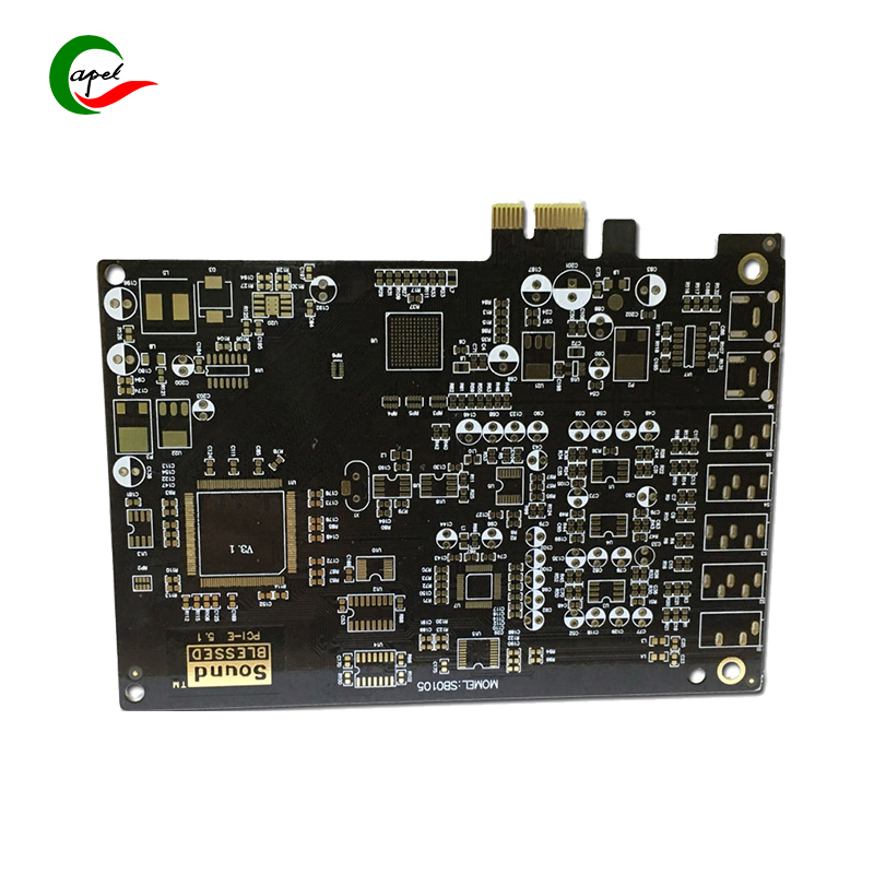
Before delving into surface finish options, it is necessary to understand what a thick copper PCB is and its specific characteristics. Generally, PCBs with copper thickness greater than 3 ounces (105 µm) are considered thick copper PCBs. These boards are designed to carry high currents and dissipate heat efficiently, which makes them suitable for power electronics, automotive, aerospace applications and other devices with high power requirements. Thick copper PCBs offer excellent thermal conductivity, higher mechanical strength and lower voltage drop than standard PCBs.
2.Importance of surface treatment in Heavy Copper Pcb Manufacturing:
Surface preparation plays a vital role in protecting copper traces and pads from oxidation and ensuring reliable solder joints. They act as a barrier between exposed copper and external components, preventing corrosion and maintaining solderability. Additionally, surface finish helps provide a flat surface for component placement and wire bonding processes. Choosing the correct surface finish for thick copper PCBs is critical to optimizing their performance and reliability.
3.Surface treatment options for Heavy Copper PCB:
Hot air solder leveling (HASL):
HASL is one of the most traditional and cost-effective PCB surface treatment options. In this process, the PCB is immersed in a bath of molten solder and the excess solder is removed using a hot air knife. The remaining solder forms a thick layer on the copper surface, protecting it from corrosion. Although HASL is a widely used surface treatment method, it is not the best choice for thick copper PCBs due to various factors. The high operating temperatures involved in this process can cause thermal stress on thick copper layers, causing warping or delamination.
Electroless nickel immersion gold plating (ENIG):
ENIG is a popular choice for surface treatment and is known for its excellent weldability and corrosion resistance. It involves depositing a thin layer of electroless nickel and then depositing a layer of immersion gold on the copper surface. ENIG has a flat, smooth surface finish, making it suitable for fine-pitch components and gold wire bonding. While ENIG can be used on thick copper PCBs, it is critical to consider the thickness of the gold layer to ensure adequate protection against high currents and thermal effects.
Electroless Nickel Plating Electroless Palladium Immersion Gold (ENEPIG):
ENEPIG is an advanced surface treatment that provides excellent solderability, corrosion resistance and wire bondability. It involves depositing a layer of electroless nickel, then a layer of electroless palladium, and finally a layer of immersion gold. ENEPIG offers excellent durability and can be applied to thick copper PCBs. It provides a rugged surface finish, making it suitable for high-power applications and fine-pitch components.
Immersion tin (ISn):
Immersion tin is an alternative surface treatment option for thick copper PCBs. It immerses the PCB in a tin-based solution, forming a thin layer of tin on the copper surface. Immersion tin provides excellent solderability, a flat surface, and is environmentally friendly. However, one consideration when using immersion tin on thick copper PCBs is that the thickness of the tin layer should be carefully controlled to ensure adequate protection against oxidation and high current flow.
Organic solderability preservative (OSP):
OSP is a surface treatment that creates a protective organic coating on exposed copper surfaces. It has good solderability and is cost effective. OSP is suitable for low to medium power applications and can be used on thick copper PCBs as long as current carrying capacity and thermal dissipation requirements are met. One of the factors to consider when using OSP on thick copper PCBs is the additional thickness of the organic coating, which may affect the overall electrical and thermal performance.
4.Things to consider when choosing a surface finish for Heavy Copper PCBs:When choosing the surface finish for a Heavy
Copper PCB, there are several factors to consider:
Current Carrying Capacity:
Thick copper PCBs are primarily used in high power applications, so it is critical to choose a surface finish that can handle high current loads without significant resistance or overheating. Options such as ENIG, ENEPIG, and immersion tin are generally suitable for high current applications.
Thermal Management:
Thick copper PCB is known for its excellent thermal conductivity and heat dissipation capabilities. The surface finish should not hinder heat transfer or cause excessive thermal stress on the copper layer. Surface treatments such as ENIG and ENEPIG have thin layers that often benefit thermal management.
Solderability:
Surface finish should provide excellent solderability to ensure reliable solder joints and proper function of the component. Options such as ENIG, ENEPIG and HASL provide reliable solderability.
Component Compatibility:
Consider the compatibility of the selected surface finish with the specific components to be mounted on the PCB. Fine pitch components and gold wire bonding may require surface treatments such as ENIG or ENEPIG.
Cost:
Cost is always an important consideration in PCB manufacturing. The cost of different surface treatments varies due to factors such as material cost, process complexity and required equipment. Evaluate the cost impact of selected surface finishes without compromising performance and reliability.
Thick copper PCBs offer unique advantages for high-power applications, and choosing the right surface finish is critical to optimizing their performance and reliability. While traditional options such as HASL may not be suitable due to thermal issues, surface treatments such as ENIG, ENEPIG, immersion tin and OSP can be considered depending on specific requirements. Factors such as current carrying capability, thermal management, solderability, component compatibility and cost should be carefully evaluated when selecting a finish for thick copper PCBs. By making smart choices, manufacturers can ensure successful manufacturing and long-term functionality of thick copper PCBs in a variety of electrical and electronic applications.
Post time: Sep-13-2023
Back


