
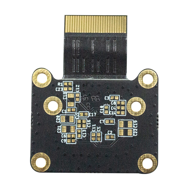
PCB (Printed Circuit Board) is an important component in modern electronic products, enabling the connections and functions of various electronic components. The PCB production process involves several key steps, one of which is depositing copper onto the substrate. This article we will look at the methods of depositing copper on PCB substrates during the production process, and delve into the different techniques used, such as electroless copper plating and electroplating.
1.Electroless copper plating: description, chemical process, advantages, disadvantages and areas of application.
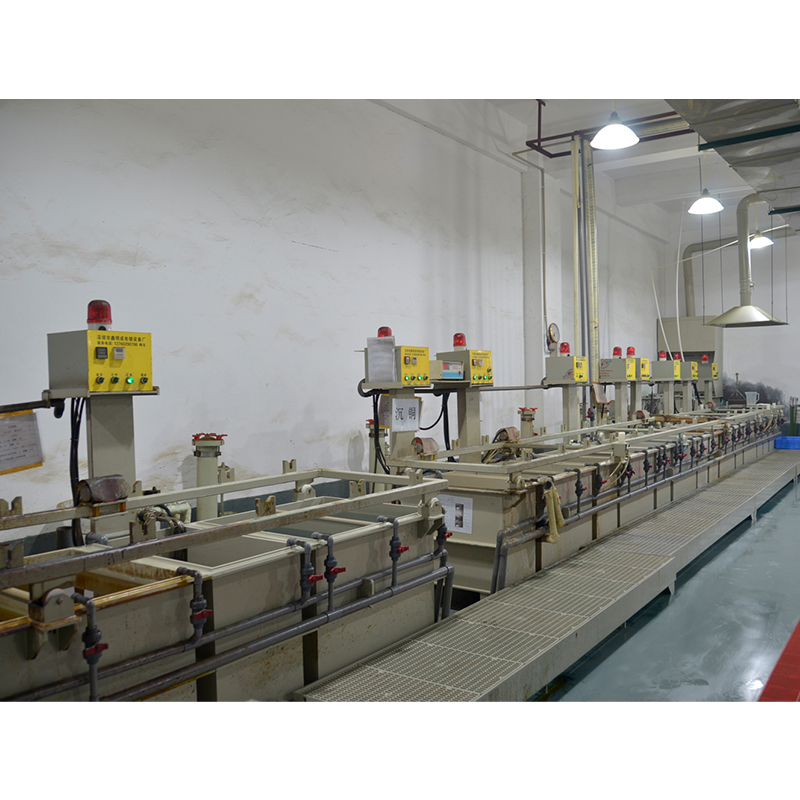
To grasp what electroless copper plating is, it is important to understand how it works. Unlike electrodeposition, which relies on electric current for metal deposition, electroless copper plating is an autophoretic process. It involves the controlled chemical reduction of copper ions on a substrate, resulting in a highly uniform and conformal copper layer.
Clean the substrate: Thoroughly clean the substrate surface to remove any contaminants or oxides that may prevent adhesion. Activation: An activation solution containing a precious metal catalyst such as palladium or platinum is used to initiate the electroplating process. This solution facilitates copper deposition onto the substrate.
Immerse in the plating solution: Immerse the activated substrate into the electroless copper plating solution. The plating solution contains copper ions, reducing agents and various additives that control the deposition process.
Electroplating process: The reducing agent in the electroplating solution chemically reduces copper ions into metallic copper atoms. These atoms then bond to the activated surface, forming a continuous and uniform layer of copper.
Rinse and dry: Once the desired copper thickness is achieved, the substrate is removed from the plating tank and rinsed thoroughly to remove any residual chemicals. Dry the plated substrate before further processing. Chemical copper plating process The chemical process of electroless copper plating involves a redox reaction between copper ions and reducing agents. Key steps in the process include: Activation: The use of noble metal catalysts such as palladium or platinum to activate the substrate surface. The catalyst provides the necessary sites for chemical bonding of copper ions.
Reducing agent: The reducing agent in the plating solution (usually formaldehyde or sodium hypophosphite) initiates the reduction reaction. These reagents donate electrons to copper ions, converting them into metallic copper atoms.
Autocatalytic reaction: The copper atoms produced by the reduction reaction react with the catalyst on the surface of the substrate to form a uniform copper layer. The reaction proceeds without the need for an externally applied current, making it “electroless plating.”
Deposition rate control: The composition and concentration of the plating solution, as well as process parameters such as temperature and pH, are carefully controlled to ensure that the deposition rate is controlled and uniform.
Advantages of electroless copper plating Uniformity: Electroless copper plating has excellent uniformity, ensuring uniform thickness in complex shapes and recessed areas. Conformal Coating: This process provides a conformal coating that adheres well to geometrically irregular substrates such as PCBs. Good adhesion: Electroless copper plating has strong adhesion to a variety of substrate materials, including plastics, ceramics and metals. Selective Plating: Electroless copper plating can selectively deposit copper onto specific areas of a substrate using masking techniques. Low Cost: Compared to other methods, electroless copper plating is a cost-effective option for depositing copper onto a substrate.
Disadvantages of electroless copper plating Slower deposition rate: Compared to electroplating methods, electroless copper plating typically has a slower deposition rate, which can lengthen the overall electroplating process time. Limited thickness: Electroless copper plating is generally suitable for depositing thin copper layers and is therefore less suitable for applications requiring thicker depositions. Complexity: The process requires careful control of various parameters, including temperature, pH and chemical concentrations, making it more complex to implement than other electroplating methods. Waste Management: Disposal of waste plating solutions containing toxic heavy metals can pose environmental challenges and requires careful handling.
Application areas of electroless copper plating PCB Manufacturing: Electroless copper plating is widely used in the manufacturing of printed circuit boards (PCBs) to form conductive traces and plated through holes. Semiconductor industry: Plays a vital role in the production of semiconductor devices such as chip carriers and lead frames. Automotive and aerospace industries: Electroless copper plating is used to make electrical connectors, switches and high-performance electronic components. Decorative and Functional Coatings: Electroless copper plating can be used to create decorative finishes on a variety of substrates, as well as for corrosion protection and improved electrical conductivity.
2.Copper plating on PCB substrate
Copper plating on PCB substrates is a critical step in the printed circuit board (PCB) manufacturing process. Copper is commonly used as an electroplating material due to its excellent electrical conductivity and excellent adhesion to the substrate. The copper plating process involves depositing a thin layer of copper on the surface of a PCB to create conductive paths for electrical signals.
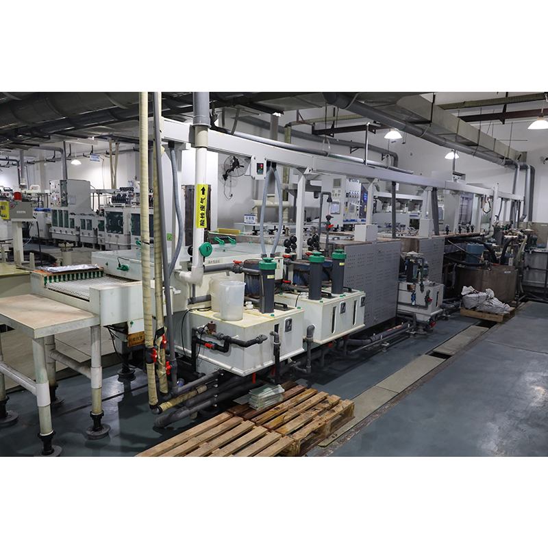
The copper plating process on PCB substrates usually includes the following steps: Surface Preparation:
Thoroughly clean the PCB substrate to remove any contaminants, oxides or impurities that may hinder adhesion and affect the quality of plating.
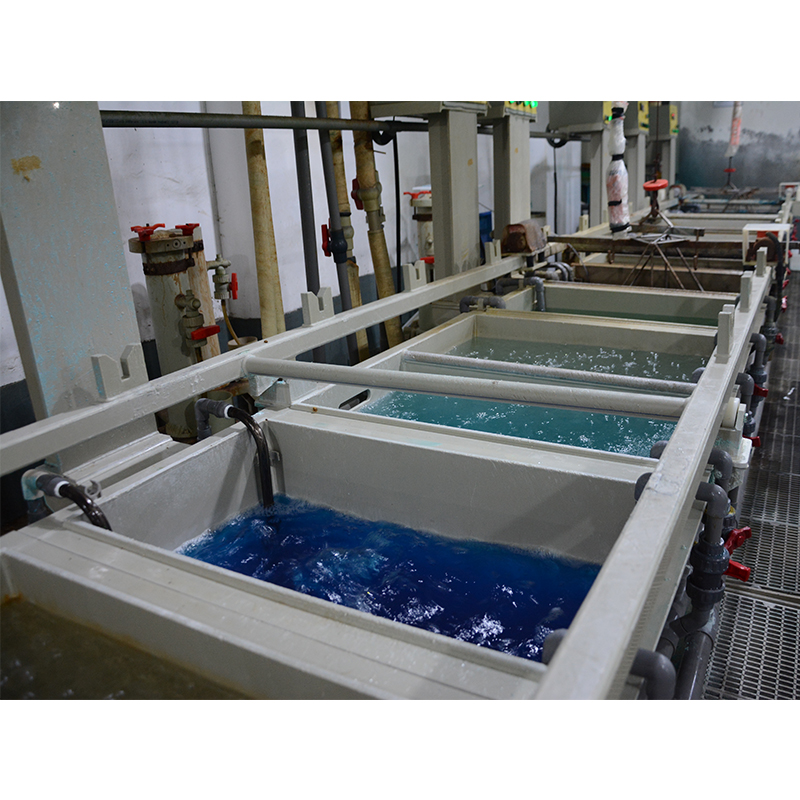
Electrolyte preparation:
Prepare an electrolyte solution containing copper sulfate as a source of copper ions. The electrolyte also contains additives that control the plating process, such as leveling agents, brighteners, and pH adjusters.
Electrodeposition:
Dip the prepared PCB substrate into the electrolyte solution and apply direct current. The PCB serves as a cathode connection, while a copper anode is also present in the solution. The current causes the copper ions in the electrolyte to be reduced and deposited onto the PCB surface.
Control of plating parameters:
Various parameters are carefully controlled during the plating process, including current density, temperature, pH, stirring and plating time. These parameters help ensure uniform deposition, adhesion, and desired thickness of the copper layer.
Post-plating treatment:
Once the desired copper thickness is reached, the PCB is removed from the plating bath and rinsed to remove any residual electrolyte solution. Additional post-plating treatments, such as surface cleaning and passivation, can be performed to improve the quality and stability of the copper plating layer.
Factors affecting electroplating quality:
Surface Preparation:
Proper cleaning and preparation of the PCB surface is critical to remove any contaminants or oxide layers and ensure good adhesion of the copper plating. Plating solution composition:
The composition of the electrolyte solution, including the concentration of copper sulfate and additives, will affect the quality of the plating. The plating bath composition should be carefully controlled to achieve the desired plating characteristics.
Plating Parameters:
Controlling plating parameters such as current density, temperature, pH, stirring and plating time is necessary to ensure uniform deposition, adhesion and thickness of the copper layer.
Substrate material:
The type and quality of PCB substrate material will affect the adhesion and quality of copper plating. Different substrate materials may require adjustments to the plating process for optimal results.
Surface roughness:
The surface roughness of the PCB substrate will affect the adhesion and quality of the copper plating layer. Proper surface preparation and control of plating parameters help minimize roughness-related problems
Advantages of PCB substrate copper plating:
Excellent electrical conductivity:
Copper is known for its high electrical conductivity, making it an ideal choice for PCB plating materials. This ensures efficient and reliable conduction of electrical signals. Excellent adhesion:
Copper exhibits excellent adhesion to a variety of substrates, ensuring a strong and long-lasting bond between the coating and the substrate.
Corrosion Resistance:
Copper has good corrosion resistance, protecting underlying PCB components and ensuring long-term reliability. Solderability: Copper plating provides a surface suitable for soldering, making it easy to connect electronic components during assembly.
Enhanced heat dissipation:
Copper is a good thermal conductor, enabling efficient heat dissipation of PCBs. This is especially important for high power applications.
Limitations and challenges of copper electroplating:
Thickness Control:
Achieving precise control over copper layer thickness can be challenging, especially in complex areas or tight spaces on the PCB. Uniformity: Ensuring uniform deposition of copper over the entire surface of a PCB, including recessed areas and fine features, can be difficult.
Cost:
Electroplating copper can be more expensive compared to other electroplating methods due to the cost of plating tank chemicals, equipment, and maintenance.
Waste Management:
Disposal of spent plating solutions and treatment of wastewater containing copper ions and other chemicals requires appropriate waste management practices to minimize environmental impact.
Process Complexity:
Electroplating copper involves multiple parameters that require careful control, requiring specialized knowledge and complex plating setups.
3.Comparison between electroless copper plating and electroplating
Performance and quality differences:
There are several differences in performance and quality between electroless copper plating and electroplating in the following aspects:
Electroless copper plating is a chemical deposition process that does not require an external power source, while electroplating involves using direct current to deposit a layer of copper. This difference in deposition mechanisms may lead to variations in coating quality.
Electroless copper plating generally provides a more uniform deposition over the entire substrate surface, including recessed areas and fine features. This is because plating occurs evenly on all surfaces regardless of their orientation. Electroplating, on the other hand, can have difficulty achieving uniform deposition in complex or hard-to-reach areas.
Electroless copper plating can achieve a higher aspect ratio (ratio of feature height to width) than electroplating. This makes it suitable for applications requiring high aspect ratio properties, such as through-holes in PCBs.
Electroless copper plating generally produces a smoother, flatter surface than electroplating.
Electroplating can sometimes result in uneven, rough or void deposits due to changes in current density and bath conditions. The quality of the bond between the copper plating layer and the substrate may vary between electroless copper plating and electroplating.
Electroless copper plating generally provides better adhesion due to the chemical bonding mechanism of electroless copper to the substrate. Plating relies on mechanical and electrochemical bonding, which can result in weaker bonds in some cases.
Cost Comparison:
Chemical Deposition vs. Electroplating: When comparing the costs of electroless copper plating and electroplating, several factors should be considered:
Chemical costs:
Electroless copper plating generally requires more expensive chemicals compared to electroplating. The chemicals used in electroless plating, such as reducing agents and stabilizers, are generally more specialized and expensive.
Equipment costs:
Plating units require more complex and expensive equipment, including power supplies, rectifiers and anodes. Electroless copper plating systems are relatively simpler and require fewer components.
Maintenance costs:
Plating equipment may require periodic maintenance, calibration, and replacement of anodes or other components. Electroless copper plating systems generally require less frequent maintenance and have lower overall maintenance costs.
Consumption of Plating Chemicals:
Plating systems consume plating chemicals at a higher rate due to the use of electrical current. The chemical consumption of electroless copper plating systems is lower because the electroplating reaction occurs through a chemical reaction.
Waste management costs:
Electroplating generates additional waste, including spent plating baths and rinse water contaminated with metal ions, which require appropriate treatment and disposal. This increases the overall cost of plating. Electroless copper plating produces less waste because it does not rely on a continuous supply of metal ions in the plating bath.
Complexities and Challenges of Electroplating and Chemical Deposition:
Electroplating requires careful control of various parameters such as current density, temperature, pH, plating time and stirring. Achieving uniform deposition and desired plating characteristics can be challenging, especially in complex geometries or low current areas. Optimization of plating bath composition and parameters may require extensive experimentation and expertise.
Electroless copper plating also requires control of parameters such as reducing agent concentration, temperature, pH and plating time. However, the control of these parameters is generally less important in electroless plating than in electroplating. Achieving the desired plating properties, such as deposition rate, thickness, and adhesion, may still require optimization and monitoring of the plating process.
In electroplating and electroless copper plating, adhesion to various substrate materials can be a common challenge. Pre-treatment of the substrate surface to remove contaminants and promote adhesion is critical for both processes.
Troubleshooting and problem solving in electroplating or electroless copper plating requires specialized knowledge and experience. Issues such as roughness, uneven deposition, voids, bubbling, or poor adhesion can occur during both processes, and identifying the root cause and taking corrective action can be challenging.
Scope of application of each technology:
Electroplating is commonly used in a variety of industries including electronics, automotive, aerospace and jewelry that require precise thickness control, high-quality finish and desired physical properties. It is widely used in decorative finishes, metal coatings, corrosion protection and electronic component manufacturing.
Electroless copper plating is mainly used in the electronics industry, especially in the manufacturing of printed circuit boards (PCBs). It is used to create conductive paths, solderable surfaces and surface finishes on PCBs. Electroless copper plating is also used to metallize plastics, produce copper interconnects in semiconductor packages, and other applications that require uniform and conformal copper deposition.
4.Copper deposition techniques for different PCB types
Single-sided PCB:
In single-sided PCBs, copper deposition is usually performed using a subtractive process. The substrate is usually made of a non-conductive material such as FR-4 or phenolic resin, coated with a thin layer of copper on one side. The copper layer serves as the conductive path for the circuit. The process begins with cleaning and preparation of the substrate surface to ensure good adhesion. Next is the application of a thin layer of photoresist material, which is exposed to UV light through a photomask to define the circuit pattern. The exposed areas of the resist become soluble and are subsequently washed away, exposing the underlying copper layer. The exposed copper areas are then etched using an etchant such as ferric chloride or ammonium persulfate. The etchant selectively removes exposed copper, leaving the desired circuit pattern. The remaining resist is then stripped off, leaving the copper traces. After the etching process, the PCB may undergo additional surface preparation steps such as solder mask, screen printing, and application of protective layers to ensure durability and protection from environmental factors.
Double-sided PCB:
A double-sided PCB has copper layers on both sides of the substrate. The process of depositing copper on both sides involves additional steps compared to single-sided PCBs. The process is similar to single-sided PCB, starting with cleaning and preparation of the substrate surface. A layer of copper is then deposited on both sides of the substrate using electroless copper plating or electroplating. Electroplating is typically used for this step because it allows better control over the thickness and quality of the copper layer. After the copper layer is deposited, both sides are coated with photoresist and the circuit pattern is defined through exposure and development steps similar to those for single-sided PCBs. The exposed copper areas are then etched to form the required circuit traces. After etching, the resist is removed and the PCB goes through further processing steps such as solder mask application and surface treatment to complete the fabrication of a double-sided PCB.
Multilayer PCB:
Multilayer PCBs are made of multiple layers of copper and insulating materials stacked on top of each other. Copper deposition in multilayer PCBs involves multiple steps to create conductive paths between the layers. The process starts with fabricating the individual PCB layers, similar to single-sided or double-sided PCBs. Each layer is prepared and a photoresist is used to define the circuit pattern, followed by copper deposition via electroplating or electroless copper plating. After deposition, each layer is coated with an insulating material (usually epoxy-based prepreg or resin) and then stacked together. The layers are aligned using precision drilling and mechanical registration methods to ensure accurate interconnection between layers. Once the layers are aligned, vias are created by drilling holes through the layers at specific points where interconnects are required. The vias are then plated with copper using electroplating or electroless copper plating to create electrical connections between the layers. The process continues by repeating the layer stacking, drilling, and copper plating steps until all required layers and interconnects are created. The final step includes surface treatment, solder mask application and other finishing processes to complete the manufacturing of the multi-layer PCB.
High Density Interconnect (HDI) PCB:
HDI PCB is a multi-layer PCB designed to accommodate high density circuitry and small form factor. Copper deposition in HDI PCBs involves advanced techniques to enable fine features and tight pitch designs. The process begins by creating multiple ultra-thin layers, often called core material. These cores have thin copper foil on each side and are made from high-performance resin materials such as BT (Bismaleimide Triazine) or PTFE (Polytetrafluoroethylene). The core materials are stacked and laminated together to create a multi-layer structure. Laser drilling is then used to create microvias, which are small holes that connect the layers. Microvias are typically filled with conductive materials such as copper or conductive epoxy. After the microvias are formed, additional layers are stacked and laminated. The sequential lamination and laser drilling process is repeated to create multiple stacked layers with microvia interconnects. Finally, copper is deposited on the surface of the HDI PCB using techniques such as electroplating or electroless copper plating. Given the fine features and high density circuitry of HDI PCBs, deposition is carefully controlled to achieve the required copper layer thickness and quality. The process ends with additional surface treatment and finishing processes to complete HDI PCB manufacturing, which may include solder mask application, surface finishing application and testing.
Flexible circuit board:
Flexible PCBs, also known as flex circuits, are designed to be flexible and able to adapt to different shapes or bends during operation. Copper deposition in flexible PCBs involves specific techniques that meet flexibility and durability requirements. Flexible PCBs can be single-sided, double-sided, or multi-layered, and copper deposition techniques vary based on design requirements. Generally speaking, flexible PCBs use thinner copper foil compared to rigid PCBs to achieve flexibility. For single-sided flexible PCBs, the process is similar to single-sided rigid PCBs, that is, a thin layer of copper is deposited on the flexible substrate using electroless copper plating, electroplating, or a combination of both. For double-sided or multi-layer flexible PCBs, the process involves depositing copper on both sides of the flexible substrate using electroless copper plating or electroplating. Taking into account the unique mechanical properties of flexible materials, deposition is carefully controlled to ensure good adhesion and flexibility. After copper deposition, the flexible PCB goes through additional processes such as drilling, circuit patterning, and surface treatment steps to create the required circuitry and complete the manufacturing of the flexible PCB.
5.Advances and Innovations in Copper Deposition on PCBs
Latest Technology Developments:Over the years, copper deposition technology on PCBs has continued to evolve and improve, resulting in increased performance and reliability. Some of the latest technological developments in PCB copper deposition include:
Advanced plating technology:
New plating technologies, such as pulse plating and reverse pulse plating, have been developed to achieve finer and more uniform copper deposition. These technologies help overcome challenges such as surface roughness, grain size and thickness distribution to improve electrical performance.
Direct metallization:
Traditional PCB manufacturing involves multiple steps to create conductive pathways, including depositing a seed layer before copper plating. The development of direct metallization processes eliminates the need for a separate seed layer, thereby simplifying the manufacturing process, reducing costs and improving reliability.
Microvia technology:
Microvias are small holes that connect different layers in a multilayer PCB. Advances in microvia technology such as laser drilling and plasma etching enable the creation of smaller, more precise microvias, enabling higher density circuits and improved signal integrity. Surface Finish Innovation: Surface finish is critical to protecting copper traces from oxidation and providing solderability. Developments in surface treatment technologies, such as Immersion Silver (ImAg), Organic Solderability Preservative (OSP), and Electroless Nickel Immersion Gold (ENIG), provide better corrosion protection, improve solderability, and increase overall reliability .
Nanotechnology and Copper Deposition: Nanotechnology plays an important role in the advancement of PCB copper deposition. Some applications of nanotechnology in copper deposition include:
Nanoparticle-based plating:
Copper nanoparticles can be incorporated into the plating solution to enhance the deposition process. These nanoparticles help improve copper adhesion, grain size and distribution, thereby reducing resistivity and enhancing electrical performance.
Nanostructured Conductive Materials:
Nanostructured materials, such as carbon nanotubes and graphene, can be integrated into PCB substrates or serve as conductive fillers during deposition. These materials have higher electrical conductivity, mechanical strength and thermal properties, thereby improving the overall performance of the PCB.
Nanocoating:
Nanocoating can be applied to the PCB surface to improve surface smoothness, solderability and corrosion protection. These coatings are often made from nanocomposites that provide better protection against environmental factors and extend the life of the PCB.
Nanoscale interconnects: Nanoscale interconnects, such as nanowires and nanorods, are being explored to enable higher density circuits in PCBs. These structures facilitate the integration of more circuits into a smaller area, allowing the development of smaller, more compact electronic devices.
Challenges and future directions: Despite significant progress, several challenges and opportunities remain to further improve copper deposition on PCBs. Some key challenges and future directions include:
Copper Fill in High Aspect Ratio Structures:
High aspect ratio structures such as vias or microvias present challenges in achieving uniform and reliable copper fill. Further research is needed to develop advanced plating techniques or alternative filling methods to overcome these challenges and ensure correct copper deposition in high aspect ratio structures.
Reducing Copper Trace Width:
As electronic devices become smaller and more compact, the need for narrower copper traces continues to grow. The challenge is to achieve uniform and reliable copper deposition within these narrow traces, ensuring consistent electrical performance and reliability.
Alternative conductor materials:
While copper is the most commonly used conductor material, alternative materials such as silver, aluminum, and carbon nanotubes are being explored for their unique properties and performance advantages. Future research may focus on developing deposition techniques for these alternative conductor materials to overcome challenges such as adhesion, resistivity, and compatibility with PCB manufacturing processes. Environmentally Friendly Processes:
The PCB industry is constantly working towards environmentally friendly processes. Future developments may focus on reducing or eliminating the use of hazardous chemicals during copper deposition, optimizing energy consumption, and minimizing waste generation to reduce the environmental impact of PCB manufacturing.
Advanced Simulation and Modeling:
Simulation and modeling techniques help optimize copper deposition processes, predict the behavior of deposition parameters, and improve the accuracy and efficiency of PCB manufacturing. Future advancements may involve integrating advanced simulation and modeling tools into the design and manufacturing process to enable better control and optimization.
6.Quality Assurance and Control of Copper Deposition for PCB Substrates
Importance of quality assurance: Quality assurance is critical in the copper deposition process for the following reasons:
Product Reliability:
The copper deposition on the PCB forms the basis for electrical connections. Ensuring the quality of copper deposition is critical to reliable and long-lasting performance of electronic devices. Poor copper deposition can lead to connection errors, signal attenuation, and overall reduced PCB reliability.
Electrical performance:
The quality of copper plating directly affects the electrical performance of PCB. Uniform copper thickness and distribution, smooth surface finish, and proper adhesion are critical to achieve low resistance, efficient signal transmission, and minimal signal loss.
Reduce costs:
Quality assurance helps identify and prevent problems early in the process, reducing the need to rework or scrap defective PCBs. This can save costs and improve overall manufacturing efficiency.
Customer Satisfaction:
Providing high-quality products is critical to customer satisfaction and building a good reputation in the industry. Customers expect reliable and durable products, and quality assurance ensures copper deposition meets or exceeds those expectations.
Testing and inspection methods for copper deposition: Various testing and inspection methods are used to ensure the quality of copper deposition on PCBs. Some common methods include:
Visual Inspection:
Visual inspection is a basic and important method of detecting obvious surface defects such as scratches, dents or roughness. This inspection can be done manually or with the help of an automated optical inspection (AOI) system.
Microscopy:
Microscopy using techniques such as scanning electron microscopy (SEM) can provide detailed analysis of copper deposition. It can carefully check the surface finish, adhesion and uniformity of the copper layer.
X-ray analysis:
X-ray analysis techniques, such as X-ray fluorescence (XRF) and X-ray diffraction (XRD), are used to measure the composition, thickness and distribution of copper deposits. These techniques can identify impurities, elemental composition, and detect any inconsistencies in copper deposition.
Electrical Testing:
Perform electrical testing methods, including resistance measurements and continuity testing, to evaluate the electrical performance of copper deposits. These tests help ensure that the copper layer has the required conductivity and that there are no opens or shorts within the PCB.
Peel Strength Test:
The peel strength test measures the bonding strength between the copper layer and the PCB substrate. It determines whether the copper deposit has sufficient bond strength to withstand normal handling and PCB manufacturing processes.
Industry standards and regulations: The PCB industry follows various industry standards and regulations to ensure the quality of copper deposition. Some important standards and regulations include:
IPC-4552:
This standard specifies the requirements for electroless nickel/immersion gold (ENIG) surface treatments commonly used on PCBs. It defines the minimum gold thickness, nickel thickness and surface quality for reliable and durable ENIG surface treatments.
IPC-A-600:
The IPC-A-600 standard provides PCB acceptance guidelines, including copper plating classification standards, surface defects and other quality standards. It serves as a reference for visual inspection and acceptance criteria of copper deposition on PCBs. RoHS Directive:
The Restriction of Hazardous Substances (RoHS) directive restricts the use of certain hazardous substances in electronic products, including lead, mercury and cadmium. Compliance with the RoHS directive ensures that copper deposits on PCBs are free of harmful substances, making them safer and more environmentally friendly.
ISO 9001:
ISO 9001 is the international standard for quality management systems. Establishing and implementing an ISO 9001-based quality management system ensures that appropriate processes and controls are in place to consistently deliver products that meet customer requirements, including the quality of copper deposition on PCBs.
Mitigating common issues and defects: Some common problems and defects that can occur during copper deposition include:
Insufficient adhesion:
Poor adhesion of the copper layer to the substrate can lead to delamination or peeling. Proper surface cleaning, mechanical roughening, and adhesion-promoting treatments can help alleviate this problem.
Uneven Copper Thickness:
Uneven copper thickness can cause inconsistent conductivity and impede signal transmission. Optimizing plating parameters, using pulse or reverse pulse plating and ensuring proper agitation can help achieve uniform copper thickness.
Voids and Pinholes:
Voids and pinholes in the copper layer can damage electrical connections and increase the risk of corrosion. Proper control of plating parameters and use of appropriate additives can minimize the occurrence of voids and pinholes.
Surface roughness:
Excessive surface roughness can negatively impact PCB performance, affecting solderability and electrical integrity. Proper control of copper deposition parameters, surface pre-treatment and post-treatment processes helps achieve a smooth surface finish.
To mitigate these issues and deficiencies, appropriate process controls must be implemented, regular inspections and tests must be conducted, and industry standards and regulations must be followed. This ensures consistent, reliable and high-quality copper deposition on the PCB. In addition, ongoing process improvements, employee training, and feedback mechanisms help identify areas for improvement and address potential issues before they become more serious.
Copper deposition on PCB substrate is a critical step in the PCB manufacturing process. Electroless copper deposition and electroplating are the main methods used, each with its own advantages and limitations. Technological advancements continue to drive innovations in copper deposition, thereby improving PCB performance and reliability. Quality assurance and control play a vital role in ensuring the production of high-quality PCBs. As the demand for smaller, faster, and more reliable electronic devices continues to increase, so does the need for precision and excellence in copper deposition technology on PCB substrates. Note: The word count of the article is approximately 3,500 words, but please note that the actual word count may vary slightly during the editing and proofreading process.
Post time: Sep-13-2023
Back


