
Introduction explores how the emergence of multilayer HDI PCBs has revolutionized the communications electronics industry
and enabled innovative advancements.
In the fast-paced field of communications electronics, innovation is the key to staying ahead. The emergence of multilayer high-density interconnect (HDI) printed circuit boards (PCBs) has revolutionized the industry, providing numerous advantages and capabilities unmatched by traditional circuit boards. From IoT devices to 5G infrastructure, multi-layer HDI PCBs play a key role in shaping the future of communications electronics.
What is Multilayer HDI PCB? Reveals the technical complexity and advanced design of multilayer HDI PCBs and their specific
relevance to high-performance electronic applications.
Multilayer HDI PCBs are technologically advanced circuit boards that feature multiple layers of conductive copper, typically sandwiched between layers of insulating substrate material. These complex circuit boards are designed for high-performance electronic applications, especially in the field of communication electronics.
Key Specifications and Material Compositions :A study of the precise specifications and material compositions that make
multilayer HDI PCBs an ideal solution for communication electronics.
Multilayer HDI PCBs used in communication electronics typically use polyimide (PI) or FR4 as the base material, plus a layer of copper and adhesive to ensure stability and performance. 0.1mm line width and spacing provide unparalleled accuracy and reliability for complex circuit designs. With a board thickness of 0.45mm +/- 0.03mm, these PCBs provide the perfect balance between compactness and ruggedness, making them ideal for space-constrained communications equipment.
The 0.1 mm minimum aperture further highlights the advanced manufacturing capabilities of multi-layer HDI PCBs, enabling the integration of densely packaged components. The presence of blind and buried vias (L1-L2, L3-L4, L2-L3) as well as plated hole fill not only facilitates complex interconnects but also enhances the overall signal integrity and reliability of the board.
Surface Treatment – Game Changer highlights the importance of electroless nickel immersion gold (ENIG) surface treatment and its impact on signal transmission and reception capabilities in communications electronics.
Electroless Nickel Immersion Gold (ENIG) surface treatment in thickness range 2-3uin provides a protective conductive coating ensuring excellent solderability and corrosion resistance. This surface treatment is of great significance in the field of communication electronics. The performance of PCB directly affects the signal transmission and reception capabilities of the device.
Applications in Communication Electronics provides an in-depth look at the various applications of multi-layer HDI PCBs in 5G
infrastructure, IoT devices and wearables, telecommunications equipment, and automotive communication systems.
One of the most striking aspects of multilayer HDI PCBs is their diverse applications in communication electronics. These PCBs are the backbone of various devices and systems, playing a key role in facilitating seamless connectivity and functionality. Let’s delve into some of the key applications where multilayer HDI PCBs are reshaping the landscape of communications electronics.
Revolutionary Impact explains how multilayer HDI PCBs are reshaping the communications electronics landscape, providing
unparalleled design flexibility, enhancing signal integrity and reliability, and driving the 5G revolution.
The evolution of 5G technology has redefined the requirements for communication infrastructure, requiring higher data transmission speeds and higher efficiency. Multi-layer HDI PCB provides an ideal platform for dense integration of components and high-speed signal transmission, which is critical to enable the deployment of 5G infrastructure. Their ability to support high-frequency and high-speed signals makes them indispensable in the manufacturing of 5G base stations, antennas and other critical components.
IoT devices and wearables
The proliferation of Internet of Things (IoT) devices and wearables requires compact yet powerful electronic components. Multilayer HDI PCBs are a catalyst for innovation in this field, facilitating the development of advanced IoT devices and wearables with their compact form factors and high-density interconnections. From smart home devices to wearable health monitors, these PCBs help bring the future of communications electronics to life.
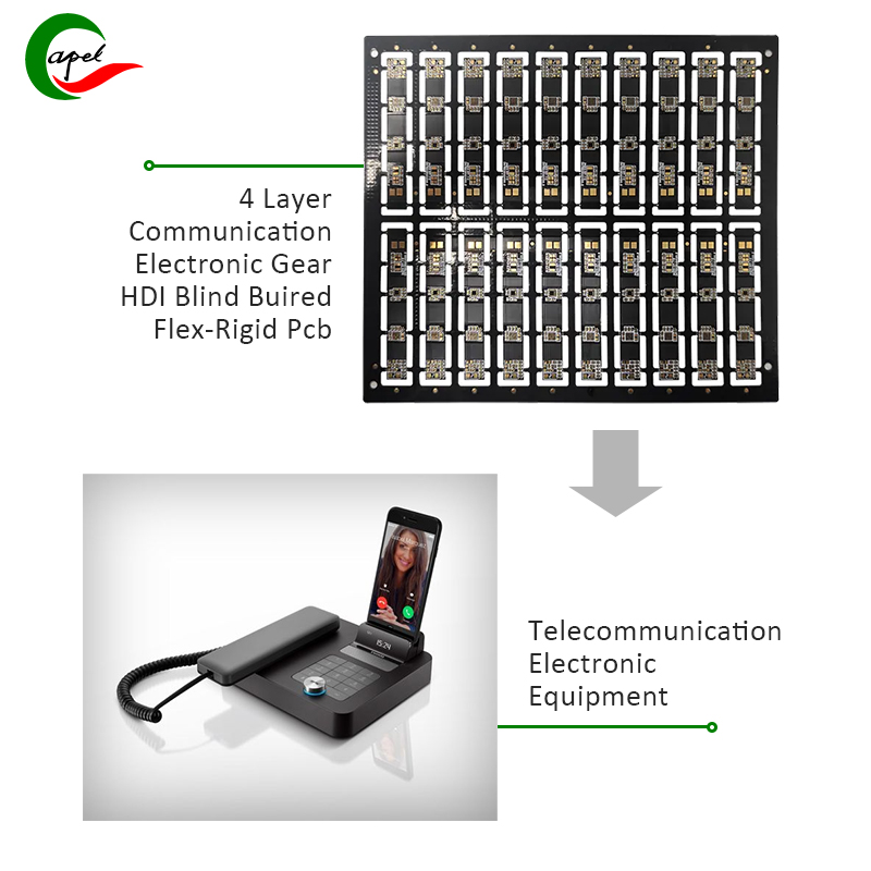
Telecommunications equipment
In the telecommunications sector where reliability and performance cannot be compromised, multi-layer HDI PCB becomes the solution of choice. By enabling seamless integration of complex communication protocols, signal processing and power management circuitry, these PCBs form the foundation for high-performance telecommunications equipment. Whether it’s a router, modem or communications server, multi-layer HDI PCBs form the backbone of these critical components.
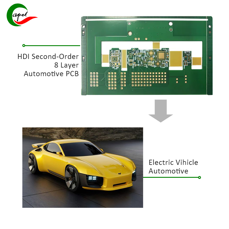
Automotive communication system
As the automotive industry undergoes a paradigm shift toward connected and autonomous vehicles, the need for robust and reliable communication systems has surged. multiple HDI PCBs are integral to realizing the vision of connected car systems, facilitating the implementation of advanced driver assistance systems (ADAS), vehicle-to-vehicle (V2V) communications and in-vehicle infotainment systems. The high-density interconnections and compact footprint provided by these PCBs help meet the stringent space and performance requirements of automotive communications electronics.
Revolutionary impact
The emergence of multi-layer HDI PCB has brought a paradigm shift in the design, manufacturing and performance of communication electronics. Their ability to support complex designs, high-frequency signals and compact form factors unlocks endless possibilities, allowing designers and engineers to push the boundaries of innovation. The role of these PCBs covers a variety of applications such as 5G infrastructure, IoT devices, telecommunications and automotive systems, and has become an integral part in shaping the future of communication electronics.
Revolutionizing Design Flexibility details how multilayer HDI PCB technology frees designers from the limitations of
traditional PCBs, allowing them to create next-generation communications devices with enhanced features and capabilities.
Multi-layer HDI circuit technology liberates designers from the constraints of traditional PCBs, providing unparalleled design flexibility and freedom. The ability to integrate multiple layers of conductive traces and vias in a compact space not only reduces the overall PCB footprint but also paves the way for complex, high-performance circuit designs. This newfound design flexibility facilitates the development of next-generation communications devices, allowing more features and functionality to be packed into smaller, more efficient form factors.
Enhanced Signal Integrity and Reliability explores the critical role of multilayer HDI PCBs in providing superior signal
integrity and minimizing signal loss, crosstalk, and impedance mismatches in communications electronics.
In the field of communication electronics, signal integrity is of paramount importance. Multilayer HDI PCBs are designed to provide superior signal integrity by minimizing signal loss, crosstalk and impedance mismatch. The combination of blind and buried vias, coupled with precise line widths and spacing, ensures that high-speed signals pass through the PCB with minimal distortion, guaranteeing reliable communications even in the most demanding applications. This level of signal integrity and reliability solidifies multilayer HDI printed circuit boards as key to modern communications electronics.
Driving the 5G Revolution reveals the integral role of multi-layer HDI PCBs in supporting high-speed, low-latency 5G network
and infrastructure deployments.
The deployment of 5G technology depends on the availability of high-performance communications infrastructure. Multilayer HDI PCBs have become the backbone of 5G infrastructure and play a key role in enabling the deployment of high-speed, low-latency networks. Their ability to support dense integration of components, high-frequency signals and complex interconnects facilitates the development of 5G base stations, antennas and other key components that form the cornerstone of 5G communications. Without the capabilities provided by multilayer HDI circuit boards, realizing the potential of 5G will remain a distant reality.
Multilayer HDI PCB Production Process
Final Thoughts, reflecting on the transformative impact of multi-layer HDI PCBs and their lasting role in shaping the future of
connectivity and communications in the digital age.
The development of communication electronics technology is intricately intertwined with the advancement of multi-layer HDI PCB technology. Not only are these PCBs redefining what is possible in design, interconnectivity and performance, they are also paving the way for transformative technologies such as 5G, IoT and connected cars. As demand for compact, high-performance communications electronics continues to surge, multilayer HDI PCBs remain at the forefront of driving innovation and driving the next wave of advancements in the field. Their transformative impact on communications electronics is undeniable, and their role in shaping the future of connectivity and communications will continue for years to come.
Post time: Jan-25-2024
Back


