
Date: 2025-07-10
In the fast-paced world of electronics and technology, efficiency is critical to maintaining a competitive advantage and meeting customer needs. High Density Interconnect (HDI) PCB prototyping and manufacturing processes play a vital role in the development and production of modern electronic devices. This article explores the importance of efficient HDI PCB prototyping and manufacturing processes and how they can help reduce time to market for electronic products.
HDI PCB, or High Density Interconnect Printed Circuit Board, is an important component in the production of modern electronic equipment. Its intricate design allows for more complex and compact electronic devices, making it an integral part of the technology industry. The prototyping process of HDI circuit board is a critical stage that directly affects the manufacturing schedule. Understanding the key steps involved in the manufacturing process is critical to achieving efficient results.
The HDI PCB manufacturing process involves several key stages, including design, material selection, layering, lamination, drilling, plating, solder mask, and surface treatment. Each step requires meticulous attention to detail and precision to ensure the final product meets the required standards and specifications.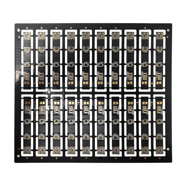
Efficient HDI PCB prototyping and making processes have many advantages and can directly shorten the time to market of electronic products. These benefits include significant reductions in development time, cost savings, improved product quality, and competitive advantages in the market.
By streamlining the prototyping and manufacturing process, companies can accelerate the development of new electronic products, allowing them to get to market faster and capitalize on emerging trends and consumer demands. Reduced development time translates directly into cost savings, as companies can bring products to market more efficiently and manage their resources effectively.
Additionally, efficient processes ensure higher product quality, as meticulous attention to detail and precision during manufacturing reduces error rates and increases reliability in the final product. This quality improvement not only benefits customers but also improves the company’s reputation and credibility in the market, thereby gaining a competitive advantage over its competitors.
To achieve an efficient HDI PCB prototyping and manufacturing process, companies can implement several strategies and best practices. These include:
A. Leverage advanced design software and tools: Using advanced design software and tools can streamline the design process, resulting in faster iteration and prototyping.
B. Work with an experienced and efficient manufacturer: Working with a reputable manufacturer with a proven track record in HDI PCB production ensures a smooth and efficient manufacturing process.
C. Implement streamlined communication and collaboration processes: Effective collaboration between design teams, manufacturing partners, and other stakeholders is critical to ensuring a seamless and efficient process from design to production.
D. Utilize automation and advanced manufacturing technologies: Automation and advanced manufacturing technologies can significantly shorten production cycles and improve overall efficiency.
Several companies have successfully reduced time to market through efficient quick turn HDI PCB prototyping and manufacturing processes. One such example is an medical Company, which implemented advanced design software and worked closely with experienced manufacturers Shenzhen Kaboer Technology Co., Ltd. to streamline its prototyping and manufacturing processes. As a result, they were able to bring their latest products to market three months early, gaining a significant competitive advantage.
In addition, Kaboer invested in automation and advanced manufacturing technology, which shortened the production cycle by 40%. Not only does this help them get their products to market faster, but it also saves significant costs and improves product quality.

Efficient HDI PCB prototyping and manufacturing processes play a vital role in shortening the time to market of electronic products. By prioritizing efficiency, companies can significantly accelerate the development and production of new electronic devices, thereby saving costs, improving product quality, and gaining a competitive advantage in the market. It is critical for companies to leverage advanced design tools, partner with experienced manufacturers, streamline communication processes, and employ automation to achieve efficient results. By doing so, companies can gain a competitive advantage and meet the changing needs of the technology industry.
In summary, now is the time for companies to prioritize efficient HDI PCB prototyping and manufacturing processes, as they are critical to gaining a competitive advantage and meeting customer expectations in today’s fast-paced technology environment. By improving efficiency, companies can not only reduce time to market but also drive innovation and success in the electronics industry.
![]()
Kaboer manufacturing PCBs since 2009. Professional technology and high-precision Printed Circuit Boards involved in Medical, IOT, UAV, Aviation, Automotive, Aerospace, Industrial Control, Artificial Intelligence, Consumer Electronics etc..


 English


 Wechat
 +86 13670210335
 +86 13670210335
 E-mail