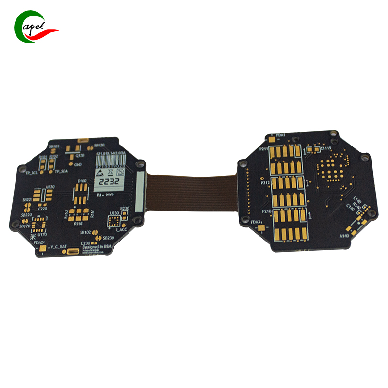
Printed circuit board (PCB) prototyping with high-speed memory interfaces can be a challenging task. Designers often face difficulties ensuring signal integrity, minimizing noise, and achieving high-speed performance. However, with the right methods and tools, it is possible to overcome these challenges and successfully prototype PCBs for high-speed memory interfaces.
In this blog post, we will explore various techniques and best practices for PCB prototyping using high-speed memory interfaces. We will discuss signal integrity, noise reduction, and the importance of selecting appropriate components. So, let’s dive into the world of high-speed memory interface prototyping!
Learn about signal integrity
Signal integrity plays a critical role in high-speed memory interface design. It refers to the quality of electrical signals passing through PCB traces and connectors. To ensure proper signal integrity, it is important to consider factors such as impedance matching, termination techniques, and controlled impedance routing.
Impedance matching is critical to preventing signal reflections that can cause data corruption and timing issues. It involves designing a transmission line with a characteristic impedance that matches the source and load impedances. Software tools such as Altium Designer and Cadence Allegro can help calculate and analyze the impedance values of critical traces.
Termination technology is used to eliminate signal reflections and ensure clean signal conversion. Popular termination techniques include series termination, parallel termination, and differential termination. The choice of termination technique depends on the specific memory interface and the required signal quality.
Controlled impedance routing involves maintaining consistent trace widths, spacing, and layer stacking to achieve a specific impedance value. This is critical for high-speed memory interfaces as it helps minimize signal degradation and maintain signal integrity.
Minimize noise
Noise is the enemy of high-speed memory interfaces. It can corrupt data, introduce errors, and degrade overall system performance. To minimize noise, proper grounding techniques, decoupling capacitors, and power supply integrity analysis are critical.
Grounding techniques include creating a solid ground plane and minimizing ground loop area. A solid ground plane helps prevent noise caused by adjacent components and reduces crosstalk. Ground loop areas should be minimized by creating single-point ground connections for all components.
Decoupling capacitors are used to absorb high-frequency noise and stabilize the power supply. Placing decoupling capacitors near high-speed memory chips and other critical components is critical to providing clean power and minimizing noise.
Power integrity analysis helps identify potential power distribution issues. Tools such as SIwave, PowerSI, and HyperLynx provide simulation capabilities to analyze the power supply network and identify areas that need modification for optimal performance.
Component selection
Choosing the right components for high-speed memory interface prototyping is critical. Components that meet strict electrical and timing requirements are critical to ensuring reliable and accurate data transmission. Key considerations when selecting components include:
1. Memory Chip: Identify memory chips designed for high-speed interfaces and provide the required capacity and performance. Popular options include DDR4, DDR5, LPDDR4 and LPDDR5.
2. Connectors: Use high-quality connectors that can handle high-speed signals without causing signal attenuation. Ensure connectors have low insertion loss, low crosstalk and excellent EMI performance.
3. Clock device: Choose a clock device that can provide a stable and accurate clock signal. PLL-based clock generators or crystal oscillators are often used for high-speed memory interfaces.
4. Passive components: Select passive components such as resistors, capacitors, and inductors that meet the requirements for impedance, capacitance, and inductance values.
Prototyping Tools and Techniques
Now that we have discussed the important considerations for designing high-speed memory interfaces, it is time to explore the prototyping tools and techniques available to PCB designers. Some widely used tools and techniques include:
1. PCB design software: Use advanced PCB design software such as Altium Designer, Cadence Allegro, or Eagle to create PCB layouts. These software tools provide high-speed design rules, impedance calculators, and simulation capabilities to ensure signal integrity.
2. High-speed test equipment: Use high-speed test equipment such as oscilloscopes, logic analyzers, and signal generators to verify and debug the memory interface design. These tools help capture and analyze signals, measure signal integrity, and identify problems.
3. PCB Manufacturing Services: Partner with reliable PCB manufacturing services that specialize in high-speed and high-density PCB manufacturing. These manufacturers ensure precision, accuracy and quality in prototype manufacturing.
4. Signal integrity simulation: Use tools such as HyperLynx, SIwave, or Cadence Sigrity to perform signal integrity simulation to verify the design, identify potential signal integrity issues, and optimize routing to minimize signal degradation.
By leveraging these tools and techniques, you can significantly increase the success rate of your high-speed memory interface prototyping efforts. Remember to iterate, test, and optimize your design for optimal performance.
In conclusion
Designing and prototyping a PCB with a high-speed memory interface can be a daunting task. However, by understanding signal integrity principles, minimizing noise, selecting appropriate components, and utilizing the right prototyping tools and techniques, you can ensure a successful implementation.
Considerations such as impedance matching, termination techniques, controlled impedance routing, proper grounding, decoupling capacitors, and power supply integrity analysis are critical to achieving signal integrity and minimizing noise. Careful component selection and cooperation with a reliable PCB manufacturer are critical to achieving a high-performance memory interface.
So, take the time to plan, design, and prototype your high-speed memory interface PCB, and you’ll be well-positioned to meet the demands of modern electronic systems. Happy prototyping!
Post time: Oct-28-2023
Back


