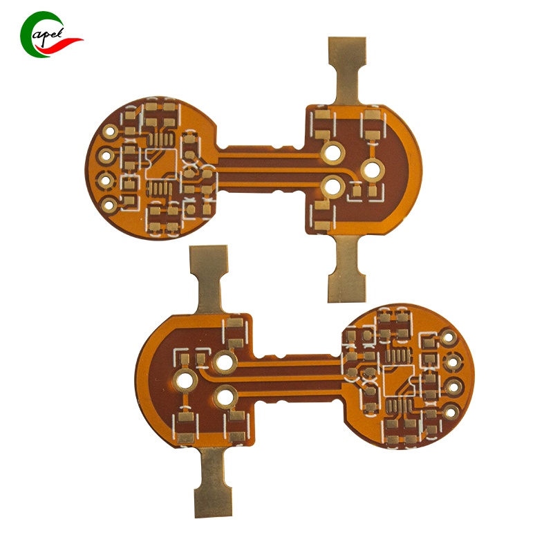
Introduce:
Prototyping a printed circuit board (PCB) for a radio frequency (RF) amplifier may seem like a complex task, but with the right knowledge and resources, it can be a rewarding process. Whether you are an electronics enthusiast or a professional engineer, this blog aims to provide a comprehensive guide on RF amplifier PCB prototyping. After reading this article, you will have a clear understanding of the steps involved and factors to consider when undertaking such a project.
1. Understand PCB prototyping:
Before delving into RF amplifier prototyping, it is necessary to have a comprehensive and in-depth understanding of PCB prototyping. A PCB is a board made of insulating material on which electronic components and their connections are mounted. Prototyping involves designing and manufacturing PCBs to test and refine circuits before mass production.
2. Basic knowledge of RF amplifiers:
RF amplifiers are critical components in a variety of electronic systems, including communications equipment, broadcast equipment, and radar systems. Before attempting to prototype a PCB for this type of application, it is important to understand the basics of RF amplifiers. RF amplifiers amplify radio frequency signals while ensuring minimal distortion and noise.
3. RF amplifier PCB design considerations:
Designing an RF amplifier PCB requires careful consideration of various factors. Some key aspects to remember are:
A. PCB Materials and Layer Stackup:
The choice of PCB materials and layer stackup has a significant impact on RF amplifier performance. Materials such as FR-4 offer cost-effective solutions for low-frequency applications, while high-frequency designs may require specialty laminates with specific dielectric properties.
b. Impedance matching and transmission lines:
Achieving impedance matching between amplifier circuit stages is critical for optimal performance. This can be achieved through the use of transmission lines and matching networks. Simulation using software tools such as ADS or SimSmith can be very helpful in designing and fine-tuning matching networks.
C. Grounding and RF Isolation:
Proper grounding and RF isolation techniques are critical to minimizing noise and interference. Considerations such as dedicated ground planes, isolation barriers, and shielding can significantly improve the performance of an RF amplifier.
d. Component layout and RF routing:
Strategic component placement and careful RF trace routing are critical to minimizing parasitic effects such as crosstalk and stray capacitance. Following best practices, such as keeping RF traces as short as possible and avoiding 90-degree trace bends, can help achieve better performance.
4. PCB prototyping method:
Depending on the complexity and requirements of the project, several methods can be used to prototype an RF amplifier PCB:
A. DIY etching:
DIY etching involves using copper clad laminates, etching solutions, and specialized transfer techniques to create a PCB. While this approach works for simple designs, it may not be ideal since RF amplifiers are sensitive to stray capacitance and impedance changes.
b. Prototyping services:
Professional PCB prototyping services provide faster and more reliable solutions. These services offer specialized equipment, quality materials and advanced manufacturing processes. Using such services can speed up RF amplifier prototyping iterations and improve accuracy.
C. Simulation tools:
Using simulation tools such as LTSpice or NI Multisim can help in the initial design phase before physical prototyping. These tools allow you to simulate the behavior of amplifier circuits, analyze performance parameters and make necessary adjustments before hardware implementation.
5. Test and iterate:
Once the PCB prototype of the RF amplifier is completed, thorough testing is critical to verify its performance. Testing may involve measuring key parameters such as gain, noise figure, linearity and stability. Depending on the results, iterative modifications may be needed to further refine the design.
6. Conclusion:
Prototyping a PCB for an RF amplifier is not a simple task, but with the proper planning, knowledge, and resources, it can be accomplished successfully. Understanding the basics of PCB prototyping, RF amplifiers, and specific design considerations is critical. Additionally, choosing appropriate prototyping methods and thorough testing will result in a fully optimized PCB design for your RF amplifier project. So don’t hesitate to embark on this exciting journey to turn your RF amplifier ideas into reality!
Ultimately, RF amplifier PCB prototyping requires a combination of technical expertise, careful design considerations, and proper prototyping methodology. By following the steps outlined in this guide, you can begin your journey to creating a high-performance RF amplifier through successful PCB prototyping.
Post time: Oct-28-2023
Back


