
Introduce
A. Company Profile: 15 years of experience in HDI PCB, HDI Flex PCB, HDI rigid-flex PCB manufacturing and prototyping
With 15 years of industry experience, our company has become a leader in High Density Interconnect (HDI) PCB, HDI Flex PCB and HDI Rigid-Flex PCB manufacturing and prototyping. Our continuous efforts to innovate and meet the ever-changing needs of the electronics industry have made the manufacturing and prototyping of multi-layer HDI PCBs the cornerstone of our expertise.
B. The importance of multi-layer HDI PCB prototyping and manufacturing in electronic devices
The need for smaller, lighter, and more complex electronic devices is driving the need for advanced printed circuit board (PCB) technologies such as multilayer HDI PCBs. These boards provide greater design flexibility, improved signal integrity and enhanced performance. As electronic devices continue to evolve, multi-layer HDI PCB prototyping and manufacturing are becoming increasingly important to meet the needs of modern technology.
What is multilayer HDI PCB?
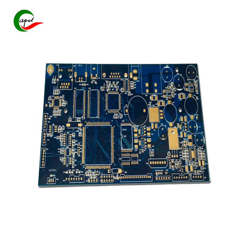
Multilayer HDI PCB refers to a printed circuit board with high-density interconnections and multi-layer wiring interconnected through microvias. These boards are designed to accommodate complex and dense electronic components, resulting in significant space and weight savings.
Benefits and Advantages of Using Multilayer HDI PCB Boards in Electronic Applications
Enhanced Signal Integrity: Multi-layer HDI PCB provides superior signal integrity due to reduced signal loss and interference, making it ideal for high-frequency applications.
Miniaturization: The compact design of multi-layer HDI PCBs enables the miniaturization of electronic devices, allowing manufacturers to develop smaller, more portable products.
Improved reliability: The use of microvias and advanced interconnect technology enhances the reliability of multi-layer HDI PCBs, helping to improve the performance and service life of electronic devices.
Applications and industries that benefit from multi-layer HDI PCB circuit board technology
Multilayer HDI PCBs are widely used in many industries, including telecommunications, automotive, aerospace, medical equipment, consumer electronics, and more. These boards are particularly suitable for high-speed and high-frequency applications where signal integrity and space constraints are critical factors.
Multilayer HDI PCB prototyping process
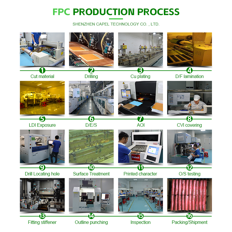
A. Step-by-step guide to multi-layer HDI PCB prototyping process
The multilayer HDI PCB prototyping process involves several key steps, including design verification, material selection, stackup planning, microvia drilling, and electrical testing. Each step plays a critical role in ensuring the prototype’s manufacturability and functionality.
B. Best practices and considerations for successful multi-layer HDI PCB prototyping
Successful multilayer HDI PCB prototyping requires careful attention to design guidelines, material selection and manufacturing processes. Adhering to best practices and considering factors such as signal integrity, thermal management, and manufacturing capabilities are critical to achieving high-quality prototypes.
C. The Importance of Working with a Reputable Manufacturer for Prototyping
Working with an experienced and reputable manufacturer for multi-layer HDI circuit boards prototyping is critical to ensuring the success of your project. Manufacturers with proven expertise can provide valuable insights, technical support and efficient prototyping services to improve product performance and accelerate time to market.
Multilayer HDI PCB manufacturing process
A. Overview of Multilayer HDI PCB Manufacturing Process
The manufacturing process of multi-layer HDI printed circuit boards involves several key stages, including design input, material preparation, imaging, drilling, plating, etching, lamination and final inspection. Each stage is carefully executed to adhere to strict quality standards and design requirements.
B. Key factors to consider for successful multi-layer HDI PCB manufacturing
Factors such as design complexity, material selection, manufacturing capabilities and quality control are important considerations for the successful manufacturing of multi-layer HDI PCBs. Optimal communication between design engineers and manufacturing experts is essential to resolve any potential challenges and ensure the production process runs smoothly.
C. Technologies and processes used in multi-layer HDI PCB manufacturing
Multilayer HDI PCBs are typically produced using advanced manufacturing techniques, including laser drilling, sequential lamination, automated optical inspection (AOI), and controlled impedance testing. These technologies enable precise manufacturing and strict quality control measures.
Choosing the Right Multilayer HDI Printed Circuit Board Prototyping and Manufacturing Manufacturer
A. Qualities that multi-layer HDI PCB proofing and manufacturing manufacturers should possess
Selecting the right manufacturer for multilayer HDI PCB prototyping and manufacturing requires evaluating key qualities such as technical expertise, manufacturing capabilities, quality assurance processes, and customer support. A trustworthy manufacturer should demonstrate a track record of successful projects and the ability to meet specific project requirements.
B. Case studies and success stories of working with reputable manufacturers
Case studies and success stories of working with reputable multilayer HDI PCB manufacturers provide valuable insights into the manufacturer’s capabilities and performance. Real-world examples can demonstrate a manufacturer’s ability to overcome challenges, deliver high-quality products, and support customer project success.
C. How to evaluate and select the best manufacturer for your multilayer HDI PCB needs
When evaluating potential manufacturers for multilayer HDI PCB prototyping and manufacturing, factors such as technical expertise, quality standards, production capabilities, lead times, and communication channels must be considered. Conducting a thorough evaluation and requesting detailed recommendations can help determine the manufacturer best suited for specific project requirements.
Multilayer HDI Printed Circuit Board Fabrication Process
In summary
A. Review of the Importance of Multilayer HDI PCBs and Prototyping/Manufacturing Processes The importance of multilayer HDI PCBs and their prototyping/manufacturing processes in meeting the ever-changing needs of modern electronic devices cannot be overstated. These boards provide the foundation for innovation and help develop advanced and compact electronic products.
B. Final Thoughts on the Impact of Working with an Experienced Manufacturer The impact of working with an experienced manufacturer for multi-layer HDI PCB prototyping and manufacturing is profound. It enables successful product design, improved performance and faster time to market.
C. Calling readers to know more about the multi-layer HDI PCB prototyping and manufacturing services offered by the company We invite readers to explore our comprehensive multi-layer HDI PCB prototyping and manufacturing services, backed by our years of experience, technical expertise, and Commitment to excellence.
By partnering with us, you can harness the power of advanced PCB technology to bring your
innovative electronic designs to life.
In summary, the importance of multilayer HDI PCB prototyping and manufacturing in today’s electronic device market cannot be overstated. As devices become smaller, lighter, and more complex, demand for advanced PCB technologies such as multilayer HDI PCBs continues to grow. By understanding the intricacies of the prototyping and manufacturing process and choosing a trusted manufacturer, companies can leverage the benefits of multilayer HDI PCBs to drive product innovation and competitive advantage in the electronics industry. We invite readers to explore our comprehensive range of multi-layer HDI PCB prototyping and manufacturing services, backed by our years of experience, technical expertise and commitment to excellence. By partnering with us, you can harness the power of advanced PCB technology to bring your innovative electronic designs to life.
Post time: Jan-16-2024
Back


