
Introduce:
In the rapidly evolving telecommunications sector, maintaining a competitive advantage requires innovation and the ability to quickly turn ideas into reality. Developing and deploying cutting-edge technologies in this field requires an efficient prototyping process, a key element of which is the design and development of printed circuit boards (PCBs). In this blog, we’ll explore the answer to the question, “Can I prototype a PCB for telecom equipment?” and dive into the steps involved in this exciting journey of change.
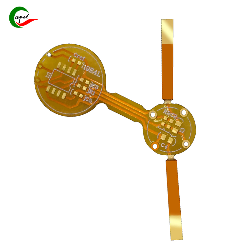
Understanding PCBs in Telecommunications:
Before discussing prototyping, it is necessary to understand the role of PCB in the telecommunications field. PCBs are the foundation upon which electronic components and systems are built. They are essential in providing connectivity and facilitating the smooth transfer of data and information. In telecommunications equipment, PCBs are used in routers, switches, modems, base stations, and even smartphones, showing their importance.
Telecom Equipment PCB Prototyping:
Telecom equipment PCB prototyping involves a step-by-step process that requires meticulous design, technical expertise, and utilization of the latest tools and techniques. Let’s take a closer look at each stage:
1. Concept:
The first step is to conceive and conceptualize the PCB design. It is important to define the goals of the PCB, understand the requirements of the device, and identify any specific needs related to telecommunications equipment. Working with a team of experts and stakeholders at this stage can provide valuable insights and help streamline the process.
2. Scheme design:
Once the concept is clear, the next step is to create the schematic design. This requires designing the circuit layout, including interconnections between the various components, and configuring the necessary power circuits. Ensuring compatibility, reliability, and compliance with industry standards is critical at this stage.
3. Circuit board layout design:
After the schematic design is completed, the circuit board layout design phase begins. This stage involves placing the components on the PCB and routing the necessary connections. It is critical to ensure proper spacing, consider signal integrity, and consider thermal management. Utilizing advanced software tools, such as AutoCAD or Altium Designer, can simplify this process and optimize the overall layout.
4. Component selection:
Choosing the right components for telecommunications equipment is fundamental to a successful prototyping process. Factors such as performance requirements, availability, cost, and compatibility with the chosen design must be considered. Working closely with parts suppliers or manufacturers is critical to sourcing reliable and high-quality parts.
5. Manufacturing and Assembly:
Once the design is complete, the virtual model can be converted into a physical PCB. Utilizing manufacturing services such as a printed circuit board assembly (PCBA) company can greatly simplify this process. These specialist companies have the expertise and equipment to manufacture and assemble functional prototypes quickly and efficiently.
6. Test and iterate:
Once the physical prototype is ready, it needs to be thoroughly tested to ensure its functionality and performance. Rigorous testing can help identify any design flaws, potential issues, or areas for improvement. Any necessary adjustments or modifications are then made, and if necessary, further iterations of the prototyping process are performed until the desired result is achieved.
Advantages of PCB prototyping for telecommunications equipment:
Telecom equipment PCB prototyping offers many advantages, including:
1. Accelerate innovation: Prototyping enables engineers and designers to bring their ideas to reality faster, promoting rapid innovation and staying ahead of competitors in a fast-paced industry.
2. Cost Optimization: Identifying potential design flaws or issues during the prototyping phase can help prevent costly mistakes during the volume production phase.
3. Improved quality: Prototyping allows designs to be tested and refined, thereby improving the overall quality, reliability, and performance of the final product.
4. Customization and flexibility: Prototyping can customize and adapt PCB designs to specific project requirements, ensuring a tailor-made solution.
In conclusion:
“Can I prototype a PCB for telecommunications equipment?” The answer to this question is a resounding yes! PCB prototyping is a key opportunity for companies and individuals in the telecommunications industry to realize their innovative ideas quickly and efficiently. By following the outlined steps and leveraging modern tools, technology, and collaboration, businesses can unlock their potential and lead the way in shaping the future of telecommunications equipment. So use your imagination and embark on a journey to create the next breakthrough in telecommunications!
Post time: Oct-26-2023
Back


