
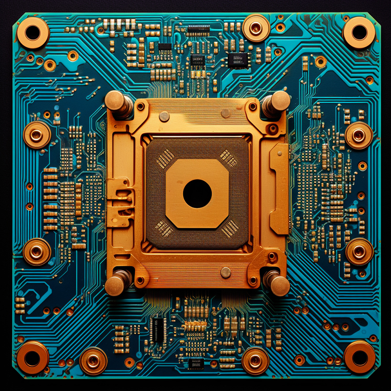
High-density interconnect (HDI) printed circuit boards (PCBs) have revolutionized the electronics industry by enabling the development of smaller, lighter, and more efficient electronic devices. With the continuous miniaturization of electronic components, traditional through-holes are no longer enough to meet the needs of modern designs. This has led to the use of microvias, blind and buried vias in HDI PCB Board. In this blog, Capel will take a deeper look at these types of vias and discuss their importance in HDI PCB design.
1. Micropore:
Microholes are small holes with a typical diameter of 0.006 to 0.15 inches (0.15 to 0.4 mm). They are commonly used to create connections between layers of HDI PCBs. Unlike vias, which pass through the entire board, microvias only partially pass through the surface layer. This allows for higher density routing and more efficient use of board space, making them crucial in the design of compact electronic devices.
Due to their small size, micropores have several advantages. First, they enable the routing of fine-pitch components such as microprocessors and memory chips, reducing trace lengths and improving signal integrity. In addition, microvias help reduce signal noise and improve high-speed signal transmission characteristics by providing shorter signal paths. They also contribute to better thermal management, as they allow thermal vias to be placed closer to heat-generating components.
2. Blind hole:
Blind vias are similar to microvias, but they extend from an outer layer of the PCB to one or more inner layers of the PCB, skipping some intermediate layers. These vias are called “blind vias” because they are only visible from one side of the board. Blind vias are mainly used to connect the outer layer of the PCB with the adjacent inner layer. Compared with through holes, it can improve wiring flexibility and reduce the number of layers.
The use of blind vias is especially valuable in high-density designs where space constraints are critical. By eliminating the need for through-hole drilling, blind vias separate signal and power planes, enhancing signal integrity and reducing electromagnetic interference (EMI) issues. They also play a vital role in reducing the overall thickness of HDI PCBs, thus contributing to the slim profile of modern electronic devices.
3. Buried hole:
Buried vias, as the name suggests, are vias that are completely hidden within the inner layers of the PCB. These vias do not extend to any outer layers and are thus “buried”. They are often used in complex HDI PCB designs involving multiple layers. Unlike microvias and blind vias, buried vias are not visible from either side of the board.
The main advantage of buried vias is the ability to provide interconnection without utilizing outer layers, enabling higher routing densities. By freeing up valuable space on the outer layers, buried vias can accommodate additional components and traces, enhancing the functionality of the PCB. They also help improve thermal management, as heat can be dissipated more effectively through the inner layers, rather than relying solely on thermal vias on the outer layers.
In conclusion, micro vias, blind vias and buried vias are key elements in HDI PCB board design and offer a wide range of advantages for miniaturization and high density electronic devices. Microvias enable dense routing and efficient use of board space, while blind vias provide flexibility and reduce layer count. Buried vias further increase routing density, freeing outer layers for increased component placement and enhanced thermal management.
As the electronics industry continues to push the boundaries of miniaturization, the importance of these vias in HDI PCB Board designs will only grow. Engineers and designers must understand their capabilities and limitations in order to utilize them effectively and create cutting-edge electronic devices that meet the ever-increasing demands of modern technology.Shenzhen Capel Technology Co., Ltd is a reliable and dedicated manufacturer of HDI printed circuit boards. With 15 years of project experience and continuous technological innovation, they are able to provide high-quality solutions that meet customer requirements. Their use of professional technical knowledge, advanced process capabilities, and advanced production equipment and testing machines ensures reliable and cost-effective products. Whether it’s prototyping or mass production, their experienced team of circuit board experts is committed to delivering first-class HDI technology PCB solutions for any project.
Post time: Aug-23-2023
Back


