
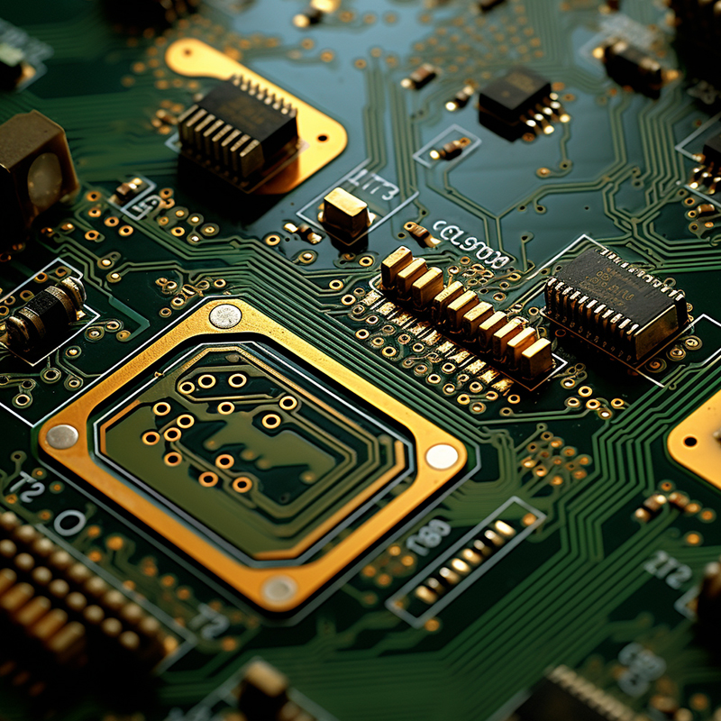
HDI (High Density Interconnect) PCBs have been a game changer in the printed circuit board world. With its compact size and advanced technology, HDI PCB has revolutionized the electronics industry in terms of functionality and efficiency. Here we will explore the main characteristics of HDI PCBs and explain why they are so widely used and sought after in modern electronic applications.
1. Miniaturization and high density:
One of the most outstanding features of HDI PCBs is their ability to achieve high component density while maintaining a compact size. This high-density interconnect technology allows more components to be placed on a smaller board area, reducing PCB size. With the growing demand for smaller, more portable electronic devices, HDI PCBs have become key to meeting the miniaturization demands of modern designs.
2. Fine pitch and microvia technology:
HDI PCB utilizes fine pitch and microvia technology to achieve higher connection density. Fine pitch means that the distance between the pad and the trace on the PCB is smaller, and small-sized components can be placed at a tighter pitch. Micropores, on the other hand, are tiny pores less than 150 microns in diameter. These microvias provide additional routing channels for interconnecting multiple layers within the HDI PCB. The combination of fine pitch and microvia technology greatly improves the overall efficiency and performance of these PCBs.
3. Improve signal integrity:
Signal integrity is a critical factor in electronic design, and HDI PCBs excel in this regard. HDI PCB size reduction and increased routing capabilities minimize signal loss and distortion, thereby enhancing signal integrity. Short trace lengths and optimized routing paths reduce the chance of signal interference, crosstalk, and electromagnetic interference (EMI). The superior signal integrity provided by HDI PCBs is critical for high-speed applications such as smartphones, tablets, and high-performance computing equipment.
4. Enhanced thermal management:
As technology continues to advance, electronic components become more powerful and generate more heat. HDI PCB is equipped with better thermal management for effective heat dissipation. The increased number of copper layers in HDI PCBs helps distribute heat evenly across the board, preventing hot spots and ensuring reliable performance. In addition, micro-via technology helps to evacuate heat from the surface layer to the inner copper plane for efficient heat dissipation.
5. Improve reliability and durability:
HDI PCBs exhibit superior reliability and durability compared to standard PCBs. Fine-pitch technology combined with precise manufacturing processes reduces the risk of opens, shorts, and other manufacturing defects. Its compact design reduces the possibility of mechanical failure due to vibration and shock. Additionally, improved thermal management prevents overheating and extends the life of electronic components, making HDI PCBs highly reliable and durable.
6. Design flexibility:
HDI PCB provides designers with greater flexibility and freedom in their designs. The compact size and high density of components opens up new possibilities for smaller, more innovative electronic devices. Fine-pitch and microvia technologies provide more routing options, enabling complex and complex designs. HDI PCBs also support blind and buried vias, allowing different layers to be interconnected without compromising usable surface area. Designers can take full advantage of these capabilities to create cutting-edge products with improved functionality and aesthetics.
HDI PCBs have become an integral part of modern electronic applications due to key features such as high density, fine pitch, microvia technology, enhanced signal integrity, thermal management capabilities, reliability, durability, and design flexibility. With the growing demand for smaller, more efficient, and more reliable electronic devices, HDI PCBs will continue to play a vital role in shaping the future of the electronics industry.
Post time: Aug-23-2023
Back


