
In today’s fast-paced technological world, electronic devices are becoming more and more advanced and compact. To meet the demands of these modern devices, printed circuit boards (PCBs) continue to evolve and incorporate new design techniques. One such technology is rigid flex pcb stackup, which offers many advantages in terms of flexibility and reliability. This comprehensive guide will explore what a rigid-flex circuit board stackup is, its benefits, and its construction.
Before diving into the details, let’s first go over the basics of PCB stackup:
PCB stackup refers to the arrangement of different circuit board layers within a single PCB. It involves combining various materials to create multilayer boards that provide electrical connections. Traditionally, with a rigid PCB stackup, only rigid materials are used for the entire board. However, with the introduction of flexible materials, a new concept emerged—rigid-flex PCB stackup.
So, what exactly is a rigid-flex laminate?
A rigid-flex PCB stackup is a hybrid circuit board that combines rigid and flexible PCB materials. It consists of alternating rigid and flexible layers, allowing the board to bend or flex as needed while maintaining its structural integrity and electrical functionality. This unique combination makes rigid-flex PCB stackups ideal for applications where space is critical and dynamic bending is required, such as wearables, aerospace equipment, and medical devices.
Now, let’s explore the benefits of choosing a rigid-flex PCB stackup for your electronics.
First, its flexibility allows the board to fit into tight spaces and conform to irregular shapes, maximizing the available space. This flexibility also reduces the overall size and weight of the device by eliminating the need for connectors and additional wiring. Additionally, the absence of connectors minimizes potential points of failure, increasing reliability. Additionally, the reduction in wiring improves signal integrity and reduces electromagnetic interference (EMI) issues.
The construction of a rigid-flex PCB stackup involves several key elements:
It usually consists of multiple rigid layers interconnected by flexible layers. The number of layers depends on the complexity of the circuit design and the desired functionality. Rigid layers typically consist of standard FR-4 or high-temperature laminates, while flexible layers are polyimide or similar flexible materials. To ensure proper electrical connection between rigid and flexible layers, a unique type of adhesive called anisotropic conductive adhesive (ACA) is used. This adhesive provides both electrical and mechanical connections, ensuring reliable performance.
To understand the structure of a rigid-flex PCB stack up, here is a breakdown of the 4-layer rigid-flex PCB board structure:
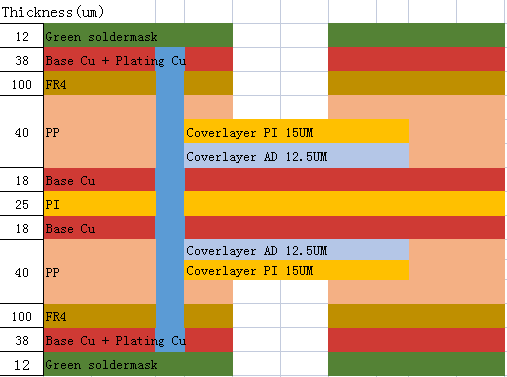
Top layer:
Green solder mask is a protective layer applied on PCB (Printed Circuit Board)
Layer 1 (Signal Layer):
Base Copper layer with Plated Copper traces.
Layer 2 (Inner Layer/dielectric layer):
FR4: This is a common insulating material used in PCBs, providing mechanical support and electrical isolation.
Layer 3 (Flex Layer):
PP: Polypropylene (PP) adhesive layer can provide protection to the circuit board
Layer 4 (Flex Layer):
Cover layer PI: Polyimide (PI) is a flexible and heat-resistant material used as a protective top layer in the flex portion of the PCB.
Cover layer AD: provide protection to the underlying material from damage by the external environment, chemicals or physical scratches
Layer 5 (Flex Layer):
Base Copper layer: Another layer of copper, typically used for signal traces or power distribution.
Layer 6 (Flex Layer):
PI: Polyimide (PI) is a flexible and heat-resistant material used as a base layer in the flex portion of the PCB.
Layer 7 (Flex Layer):
Base Copper layer: Yet another layer of copper, typically used for signal traces or power distribution.
Layer 8 (Flex Layer):
PP: Polypropylene (PP) is a flexible material used in the flex portion of the PCB.
Cowerlayer AD: provide protection to the underlying material from damage by the external environment, chemicals or physical scratches
Cover layer PI: Polyimide (PI) is a flexible and heat-resistant material used as a protective top layer in the flex portion of the PCB.
Layer 9 (Inner Layer):
FR4: Another layer of FR4 is included for additional mechanical support and electrical isolation.
Layer 10 (Bottom Layer):
Base Copper layer with Plated Copper traces.
Bottom layer:
Green soldermask.
Please note that for a more accurate assessment and specific design considerations, it is recommended to consult with a PCB designer or manufacturer who can provide detailed analysis and recommendations based on your specific requirements and constraints.
In summary:
Rigid flex PCB stackup is an innovative solution that combines the advantages of rigid and flexible PCB materials. Its flexibility, compactness and reliability make it suitable for various applications requiring space optimization and dynamic bending. Understanding the basics of rigid-flex stackups and their construction can help you make informed decisions when designing and manufacturing electronic devices. As technology continues to advance, the demand for rigid-flex PCB stackup will undoubtedly increase, driving further development in this field.
Post time: Aug-24-2023
Back


