
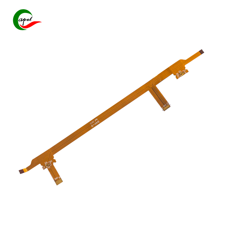
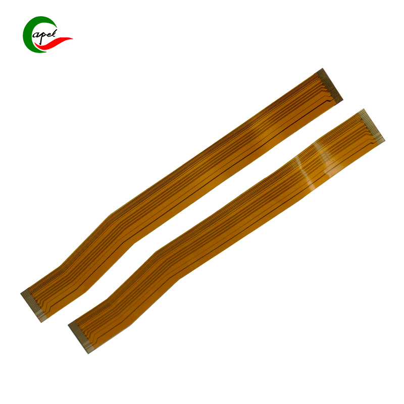
Single-Sided Flexible PCBs Supplier China PCB Prototype


Specification
| Category | Process Capability | Category | Process Capability |
| Production Type | Single layer FPC / Double layers FPC Multi- layer FPC / Aluminum PCBs Rigid-Flex PCBs |
Layers Number | 1-16 layers FPC 2-16 layers Rigid-FlexPCB HDI Printed Circuit Boards |
| Max Manufacture Size | Single layer FPC 4000mm Doulbe layers FPC 1200mm Multi-layers FPC 750mm Rigid-Flex PCB 750mm |
Insulating Layer Thickness |
27.5um /37.5/ 50um /65/ 75um / 100um / 125um / 150um |
| Board Thickness | FPC 0.06mm - 0.4mm Rigid-Flex PCB 0.25 - 6.0mm |
Tolerance of PTH Size |
±0.075mm |
| Surface Finish | Immersion Gold/Immersion Silver/Gold Plating/Tin Plat ing/OSP |
Stiffener | FR4 / PI / PET / SUS / PSA/Alu |
| Semicircle Orifice Size | Min 0.4mm | Min Line Space/ width | 0.045mm/0.045mm |
| Thickness Tolerance | ±0.03mm | Impedance | 50Ω-120Ω |
| Copper Foil Thickness | 9um/12um / 18um / 35um / 70um/100um | Impedance Controlled Tolerance |
±10% |
| Tolerance of NPTH Size |
±0.05mm | The Min Flush Width | 0.80mm |
| Min Via Hole | 0.1mm | Implement Standard |
GB / IPC-650 / IPC-6012 / IPC-6013II / IPC-6013III |
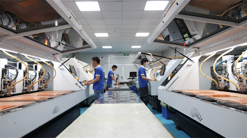
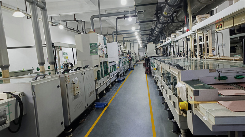
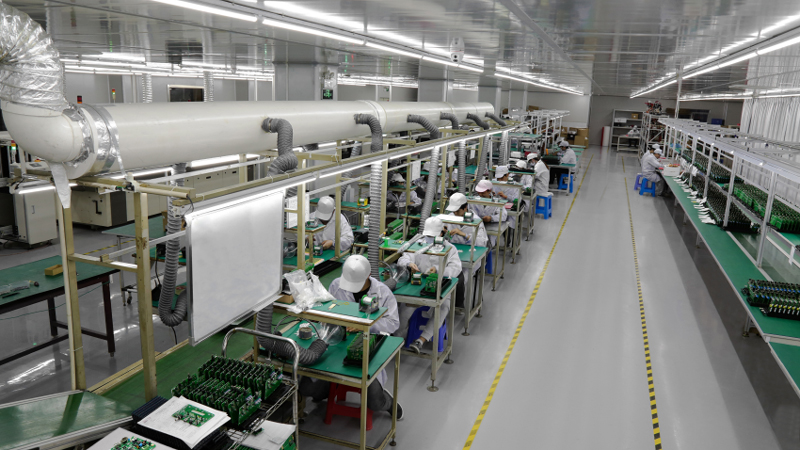
We do PCB Prototype with 15 years' experience with our professionalism
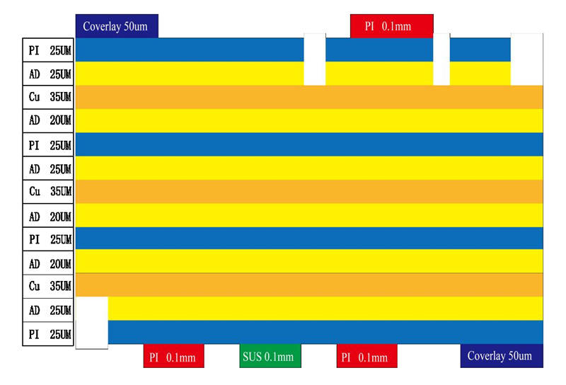
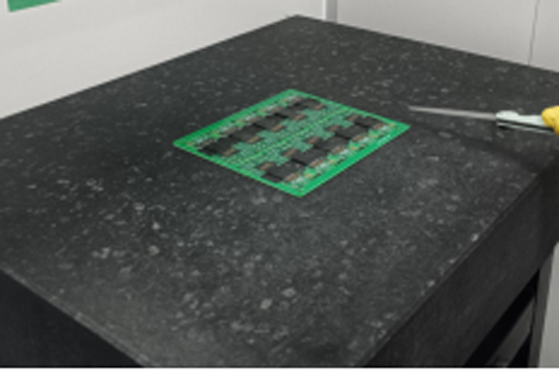
3 layer Flex PCBs
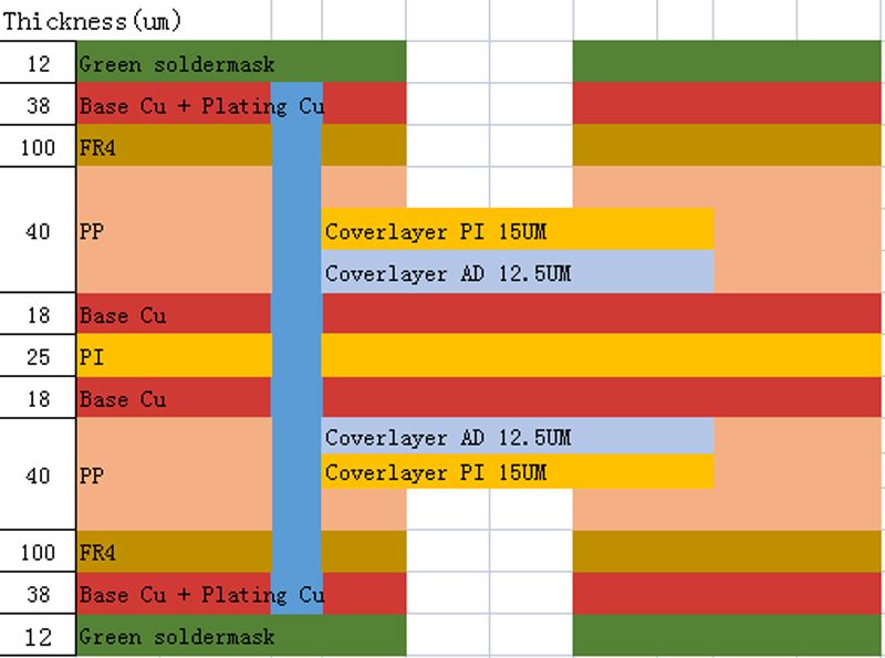
4 layer Rigid-Flex PCBs
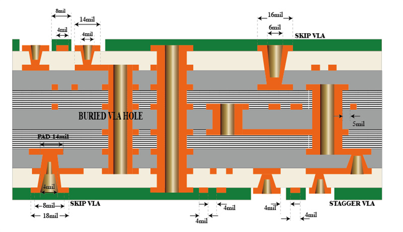
8 layer HDI Printed Circuit Boards
Testing and Inspection Equipment
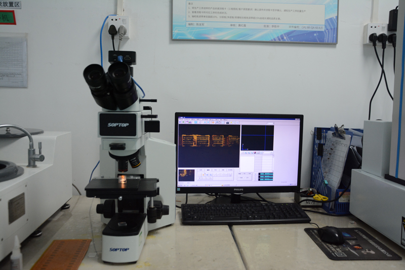
Microscope Testing
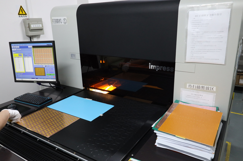
AOI Inspection
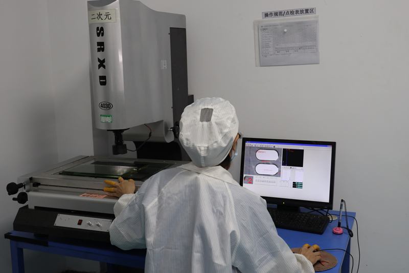
2D Testing
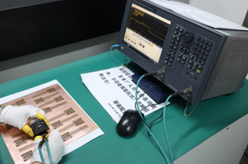
Impedance Testing
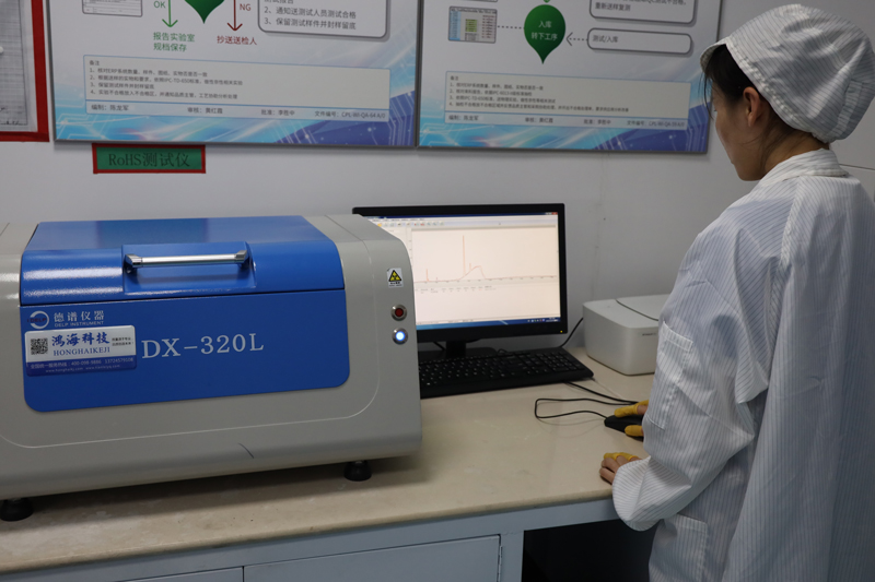
RoHS Testing
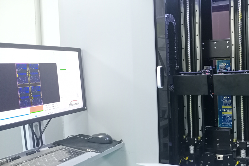
Flying Probe
Horizontal Tester
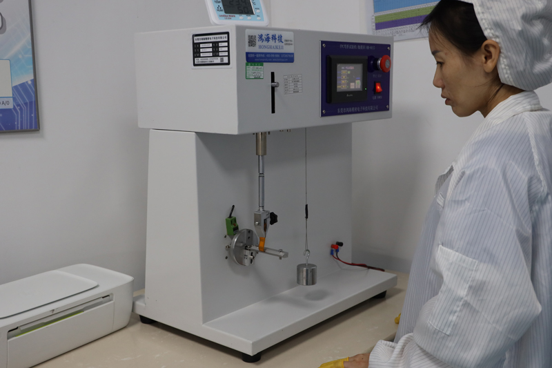
Bending Teste
Our PCB Prototype Service
. Provide technical support Pre-sales and after-sales;
. Custom up to 40 layers, 1-2days Quick turn reliable prototyping, mass production, Component procurement, SMT Assembly;
. Caters to both Medical Device, Industrial Control, Automotive, Aviation, Consumer Electronics, IOT, UAV, Communications etc..
. Our teams of engineers and researchers are dedicated to fulfilling your requirements with precision and professionalism.
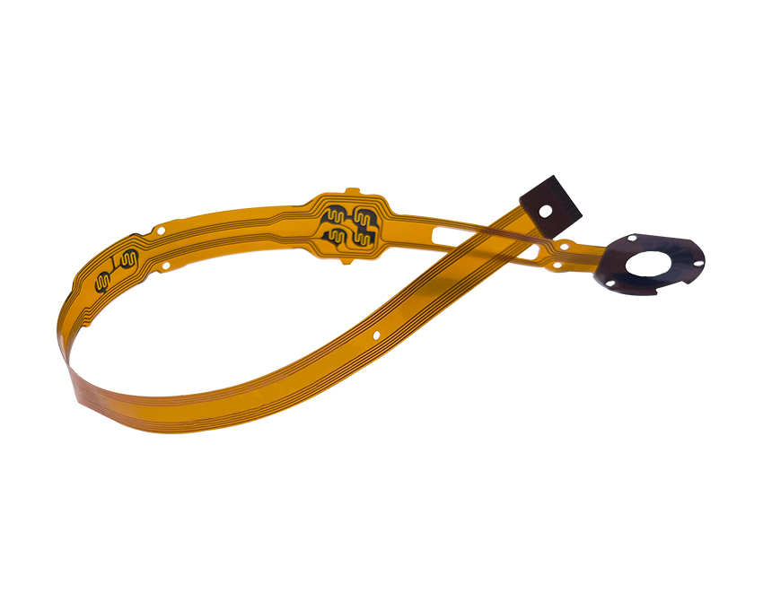
What are the technical differences between Single-side Flexible PCB and double-sided flexible circuit boards?
Single-side Flexible PCBs have a conductive layer on one side of the substrate material. Components are usually mounted on this side, while the other side remains non-conductive. Conductive traces are usually made of copper and can be made using various fabrication techniques such as etching.
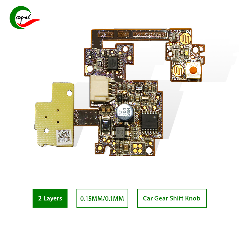
Double-sided flexible circuit boards, on the other hand, have conductive layers on both sides of the substrate.
This allows components to be mounted on both sides, increasing the overall component density and functionality of the board. Conductive traces can be interconnected using plated through holes (PTHs) or vias, allowing electrical connections between the top and bottom layers.
Another key difference is that Single-side Flexible PCB is generally more cost-effective and simpler to manufacture than double-sided. Due to the extra conductive layer and the possible use of PTH or vias, double-sided flex is usually more complex, requires a more advanced manufacturing process, and is therefore slightly more expensive.
Why need Quick-turn PCB Prototype?
1. Cost-effective small-scale production: Quick-turn PCB prototype allows for low-volume production runs, which can be cost-effective for early-stage product launches, niche markets, or limited production requirements.
It eliminates the need for large upfront investments in mass production equipment, tooling, and inventory.
2. Collaboration and feedback: Rapid PCB prototype enables engineers to collaborate with stakeholders, including customers, design teams, and manufacturers, more effectively. By having physical prototypes in hand, they can gather valuable feedback and input from various perspectives, leading to better design refinements and final product outcomes.
3. Reduced time to market: With quick-turn PCB prototype, engineers can significantly reduce the product development cycle, shortening the time it takes to bring a product to market. This enables businesses to capitalize on market opportunities, stay ahead of competitors, and generate revenue faster.
4. Flexibility in design changes: PCB Prototype offers the flexibility to incorporate design changes and improvements throughout the development process. Engineers can quickly modify and iterate on the PCB design, making adjustments based on testing results, customer feedback, or manufacturability constraints. This agility helps optimize the final product design, enhancing its performance and functionality.
5. Enhanced communication with manufacturers: Quick-turn PCB prototype involves working closely with PCB manufacturers, fostering better communication and collaboration between design teams and suppliers. This close partnership facilitates design for manufacturability (DFM), where engineers can optimize the design to ensure smooth manufacturing and avoid production issues or delays.
6. Learning and skill development: PCB Prototype allows engineers to gain valuable hands-on experience in PCB assembly and manufacturing processes. It helps them understand the complexities and nuances of PCB production, leading to improved design decisions, better DFM practices, and enhanced overall engineering skills.
-

Advanced 4 layer FPC Flex Boards fabrication Fa...
-

Auto Light LED PCB | fog lamp rigid flex pcb | ...
-

Fast Turn 4 layer FPC PCB Boards Production Com...
-
Car Wiper Flexible PCB | Car FPC | Automotive w...
-

FR4 Printed Circuit Boards Custom Multilayer Fl...
-
Quick Turn Pcb Fab Multilayer Flexible Pcb ENIG...


