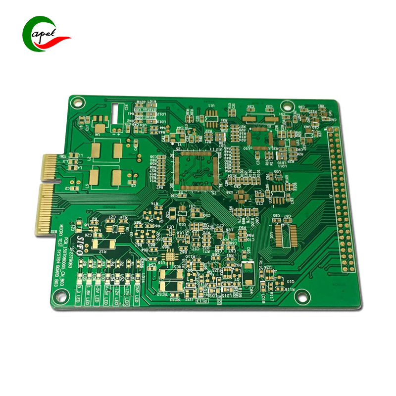
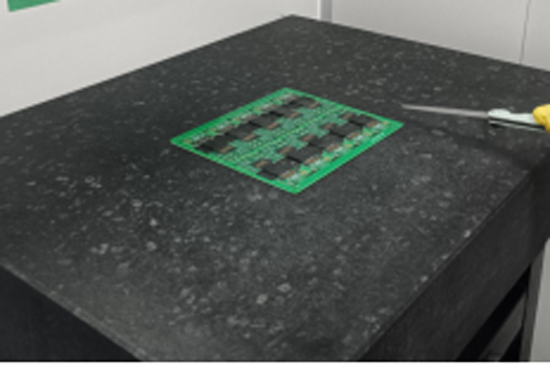
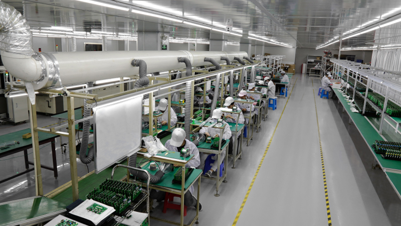
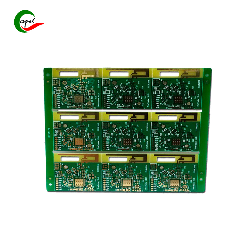
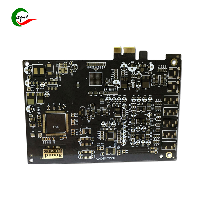
6 Layer PCB Circuit Boards Rapid Pcb Prototyping Pcb Manufacturer China
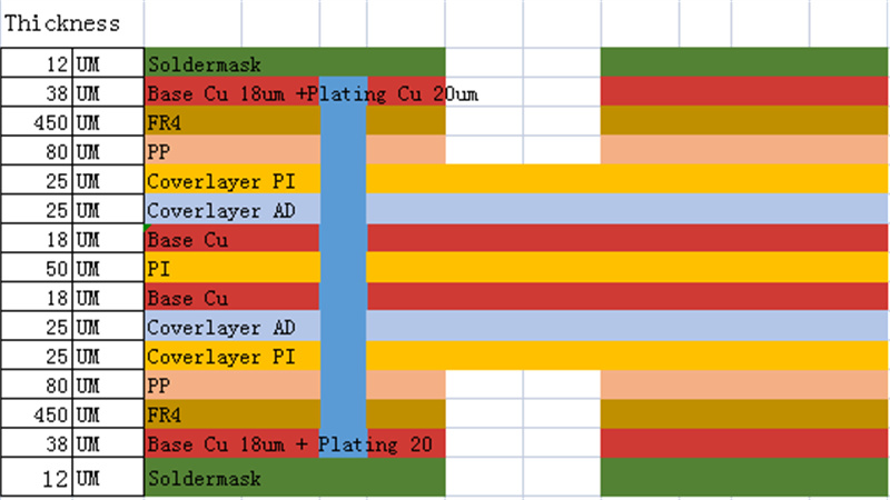
PCB Process Capability
| No. | Project | Technical indicators |
| 1 | Layer | 1-60(layer) |
| 2 | Maximum processing area | 545 x 622 mm |
| 3 | Minimumboardthickness | 4(layer)0.40mm |
| 6(layer) 0.60mm | ||
| 8(layer) 0.8mm | ||
| 10(layer)1.0mm | ||
| 4 | Minimum line width | 0.0762mm |
| 5 | Minimum spacing | 0.0762mm |
| 6 | Minimum mechanical aperture | 0.15mm |
| 7 | Hole wall copper thickness | 0.015mm |
| 8 | Metallized aperture tolerance | ±0.05mm |
| 9 | Non-metallized aperture tolerance | ±0.025mm |
| 10 | Hole tolerance | ±0.05mm |
| 11 | Dimensional tolerance | ±0.076mm |
| 12 | Minimum solder bridge | 0.08mm |
| 13 | Insulation resistance | 1E+12Ω(normal) |
| 14 | Plate thickness ratio | 1:10 |
| 15 | Thermal shock | 288 ℃(4 times in 10 seconds) |
| 16 | Distorted and bent | ≤0.7% |
| 17 | Anti-electricity strength | >1.3KV/mm |
| 18 | Anti-stripping strength | 1.4N/mm |
| 19 | Solder resist hardness | ≥6H |
| 20 | Flame retardancy | 94V-0 |
| 21 | Impedance control | ±5% |
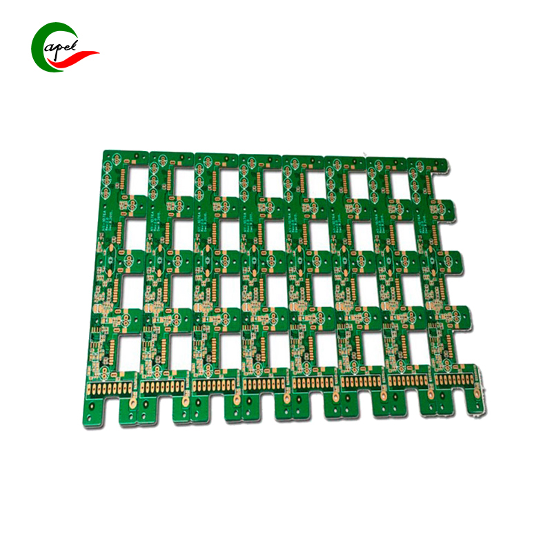
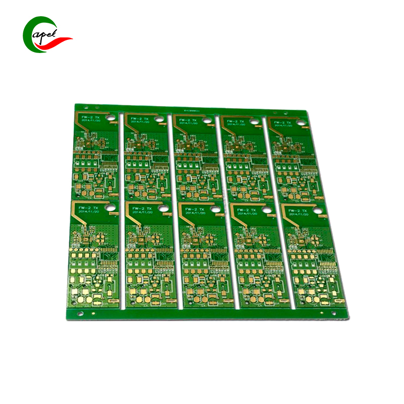
We do PCB circuit boards prototype with 15 years' experience with our professionalism
4 layer Flex-Rigid Boards
8 layer Rigid-Flex PCBs
8 layer HDI PCBs
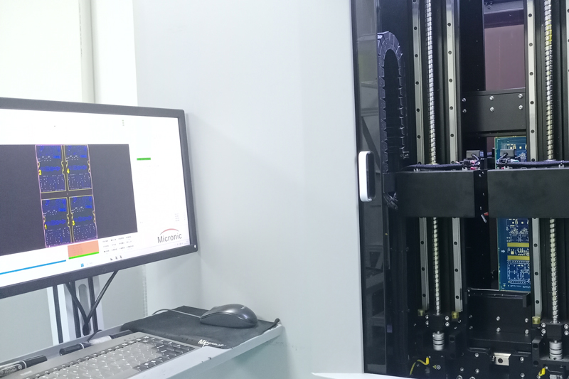
Testing and Inspection Equipment
Microscope Testing
AOI Inspection
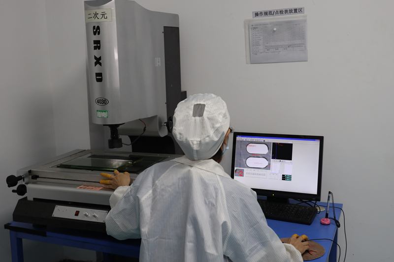
2D Testing
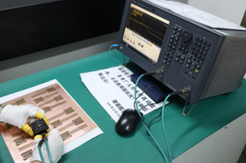
Impedance Testing
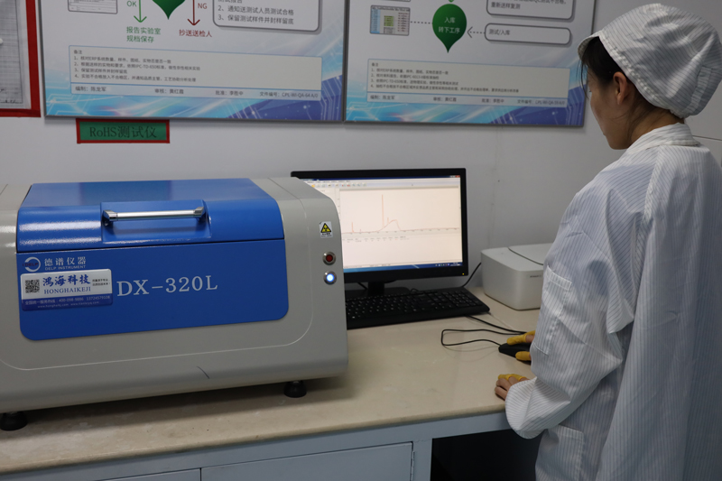
RoHS Testing
Flying Probe
Horizontal Tester
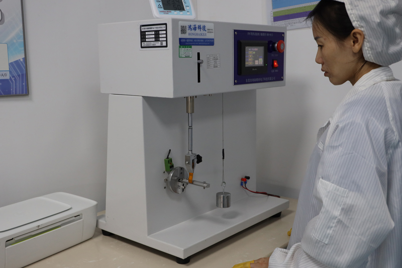
Bending Teste
Our PCB circuit boards prototype Service
. Provide technical support Pre-sales and after-sales;
. Custom up to 40 layers, 1-2days Quick turn reliable prototyping, Component procurement, SMT Assembly;
. Caters to both Medical Device, Industrial Control, Automotive, Aviation, Security, IOT, UAV, Communications etc..
. Our teams of engineers and researchers are dedicated to fulfilling your requirements with precision and professionalism.

How to choose an experienced and strong manufacturer for proofing 6-layer circuit boards.
1. Refer to word-of-mouth and evaluation: understand other customers' evaluation and word-of-mouth about the manufacturer.
Relevant information can be obtained by searching online forums, social media or professional platforms for reviews and feedback. Look for those with a solid reputation and years of experience.
2. Experience and expertise: Make sure the manufacturer has rich experience and expertise in the manufacture of 6-layer circuit boards.
Learn about their history and background, including how long they have been in the industry and the number of projects they have completed.
3. Technical capabilities and equipment: Check whether the manufacturer has advanced equipment and technology to manufacture 6-layer circuit boards.
Learn about their capabilities to manufacture complex boards and high-density assemblies to ensure they can meet your requirements.
4. Quality control: Understand the manufacturer's quality control system and process. Do they have strict quality control standards and proper testing equipment to ensure product quality, such as whether to implement ISO 9001 quality management system.
5. Reliability and deliverability: Assess the supplier's reliability and deliverability. Are they able to complete projects on time and provide accurate delivery times. Ask if they have an emergency backup plan in case of delays or unexpected events.
6. Talk to existing customers: If possible, talk to existing customers of the supplier. Learn about their cooperation experience and satisfaction, as well as the manufacturer's working attitude and response speed.
7. Interview or communicate with manufacturers: conduct interviews or communicate with potential manufacturers, and ask them about proofing requirements and technical requirements. Observe whether their answers and explanations are accurate, professional, and satisfactory, so as to judge whether they have the experience and strength you need.
8. Price and service: Finally, consider the price and after-sales service comprehensively. Make sure the price is reasonable and provide proper after-sales support, such as technical consultation, production tracking and problem solving, etc.
The proofing process of a 6 layer PCB circuit boards
1. Design the circuit schematic diagram and layout: firstly design the circuit schematic diagram and layout according to the circuit design requirements. This is a critical step in determining board dimensions, routing rules, device placement, and more.
2. Make circuit board files: Use PCB design software to convert circuit schematics and layouts into circuit board files.
These files usually include Gerber files, drill files, soldermask files, etc.
3. Verify the design: Before the circuit board is manufactured, the circuit design is verified. Ensure that your board design is free from errors and manufacturability issues by performing circuit simulation and DFM (Design for Manufacturability) analysis.
4. Submit order: Submit the board documents and corresponding manufacturing requirements to the board manufacturer. It is usually necessary to provide file format, circuit board material, number of layers, pad requirements, solder mask color, silk screen requirements, process requirements, etc.
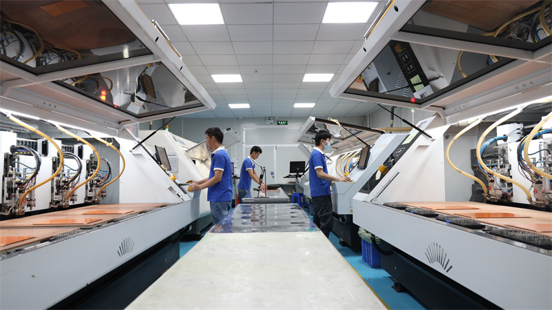
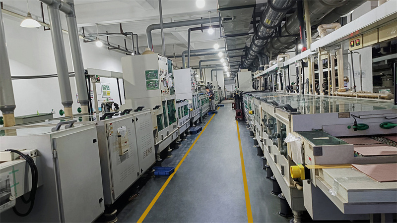
5. Manufacture circuit board: The circuit board manufacturer produces according to the documents provided.
This includes using thin films to create printed circuit board patterns, chemical etching or machining to remove unwanted copper layers, drilling, copper plating, overlays (pads, soldermask, silkscreen), dicing and other processes.
6. Carry out functional test: Carry out functional test on the manufactured single board to ensure its normal operation.
7. Assemble the circuit board: install the circuit board into the corresponding equipment for functional test or practical application.
8. Evaluate the proofing results: After receiving the proofing circuit board, conduct a comprehensive evaluation.
Check whether the appearance and size of the circuit board meet the requirements, check the pad and welding quality, and test whether the performance and function of the circuit board are normal.
9. Modification and optimization: Make necessary modification and optimization according to the evaluation results.
If the circuit board is found to have problems or needs to be improved, the design files can be modified accordingly.
10. Re-proofing: If the circuit board has a large amount of modification or multiple iterations are required, re-proofing can be carried out.
Repeat the previous process, submit the file to the factory for production again, and evaluate and revise again.
11. Mass production: When the design and performance of the circuit board are satisfactory, mass production can be carried out. Manufacturers produce according to the final design files, and produce large quantities of circuit boards to supply to customers.
12. Track and manage the supply chain: It is very important to track and manage the supply chain throughout the proofing and mass production process.
Guarantee the supply of materials, timely update the production progress, logistics arrangements, etc., and ensure the on-time delivery of circuit boards.