
Due to its complex structure and unique characteristics, the production of rigid-flex boards requires special manufacturing processes. In this blog post, we will explore the various steps involved in manufacturing these advanced rigid flexible PCB boards and illustrate the specific considerations that must be taken into consideration.
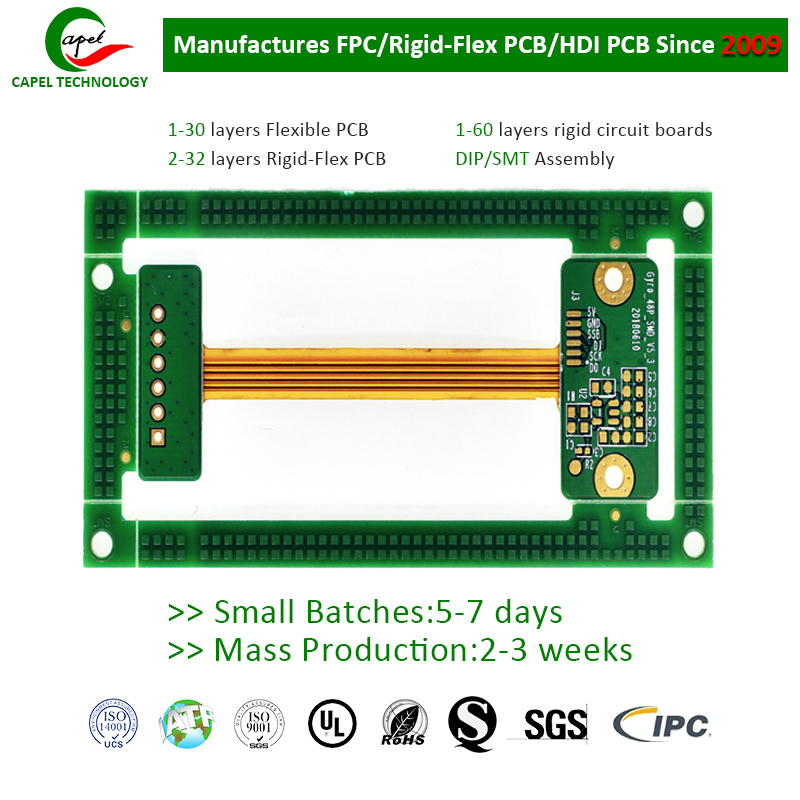
Printed circuit boards (PCBs) are the backbone of modern electronics. They are the basis for interconnected electronic components, making them an essential part of numerous devices we use every day. As technology advances, so does the need for more flexible and compact solutions. This has led to the development of rigid-flex PCBs, which offer a unique combination of rigidity and flexibility on a single board.
Design rigid-flexible board
The first and most important step in the rigid-flex manufacturing process is design. Designing a rigid-flex board requires careful consideration of the overall circuit board layout and component placement. Flex areas, bend radii and fold areas should be defined during the design phase to ensure proper functionality of the finished board.
The materials used in rigid-flex PCBs must be carefully selected to meet the specific requirements of the application. The combination of rigid and flexible parts requires that the materials selected have a unique combination of flexibility and rigidity. Typically flexible substrates such as polyimide and thin FR4 are used, as well as rigid materials such as FR4 or metal.
Layer Stacking and Preparing the Substrate for rigid flex pcb manufacturing
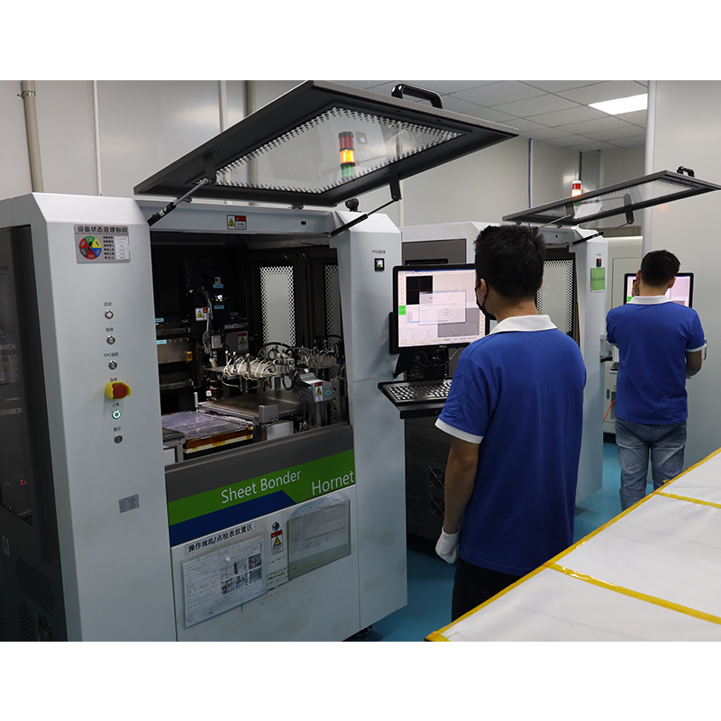
Once the design is complete, the layer stacking process begins. Rigid-flex printed circuit boards consist of multiple layers of rigid and flexible substrates that are bonded together using specialized adhesives. This bonding ensures that the layers remain intact even under challenging conditions such as vibration, bending and temperature changes.
The next step in the manufacturing process is to prepare the substrate. This includes cleaning and treating the surface to ensure optimal adhesion. The cleaning process removes any contaminants that might hinder the bonding process, while the surface treatment enhances the adhesion between the different layers. Techniques such as plasma treatment or chemical etching are often used to achieve the desired surface properties.
Copper patterning and inner layer formation for rigid flexible circuit boards facbrication
After preparing the substrate, proceed to the copper patterning process. This involves depositing a thin layer of copper on a substrate and then performing a photolithography process to create the desired circuit pattern. Unlike traditional PCBs, rigid-flex PCBs require careful consideration of the flexible portion during the patterning process. Special care must be taken to avoid unnecessary stress or damage to the flexible parts of the circuit board.
Once copper patterning is complete, inner layer formation begins. In this step, the rigid and flexible layers are aligned and the connection between them is established. This is usually accomplished through the use of vias, which provide electrical connections between different layers. Vias must be carefully designed to accommodate the flexibility of the board, ensuring they do not interfere with overall performance.
Lamination and outer layer formation for rigid-flex pcb manufacturing
Once the inner layer is formed, the lamination process begins. This involves stacking the individual layers and subjecting them to heat and pressure. Heat and pressure activate the adhesive and promote the bonding of the layers, creating a strong and durable structure.
After lamination, the outer layer formation process begins. This involves depositing a thin layer of copper on the outer surface of the circuit board, followed by a photolithography process to create the final circuit pattern. Formation of the outer layer requires precision and accuracy to ensure correct alignment of the circuit pattern with the inner layer.
Drilling, plating and surface treatment for rigid flexible pcb boards production
The next step in the manufacturing process is drilling. This involves drilling holes in the PCB to allow components to be inserted and electrical connections to be made. Rigid-flex PCB drilling requires specialized equipment that can accommodate different thicknesses and flexible circuit boards.
After drilling, electroplating is performed to enhance the conductivity of the PCB. This involves depositing a thin layer of metal (usually copper) on the walls of the drilled hole. Plated holes provide a reliable method of establishing electrical connections between different layers.
Finally, surface finishing is performed. This involves applying a protective coating to exposed copper surfaces to prevent corrosion, enhance solderability, and improve the overall performance of the board. Depending on the specific requirements of the application, different surface treatments are available, such as HASL, ENIG or OSP.
Quality control and testing for rigid flex printed circuit board manufacturing
Throughout the entire manufacturing process, quality control measures are implemented to ensure the highest standards of reliability and performance. Use advanced testing methods such as automated optical inspection (AOI), X-ray inspection and electrical testing to identify any potential defects or issues in the finished circuit board. In addition, rigorous environmental and reliability testing is performed to ensure that rigid-flex PCBs can withstand challenging conditions.
To sum up
The production of rigid-flex boards does require special manufacturing processes. The complex structure and unique characteristics of these advanced circuit boards require careful design considerations, precise material selection and customized manufacturing steps. By following these specialized manufacturing processes, electronics manufacturers can harness the full potential of rigid-flex PCBs and bring new opportunities for innovative, flexible and compact electronic devices.
Post time: Sep-18-2023
Back


